
An Optical Module project should start with form factor, reach, laser structure, thermal path, substrate routing, and test logic, not only a speed target. DEEPETCH works across high-speed optical modules, liquid cooling solutions, AOC, ceramic packages, IC packaging substrates, IDM services, EMS&PCBA/SMT, satellite communication, radar products, and TR transceiver modules. For engineers building high-speed optical transceiver EMS projects, DEEPETCH’s butterfly packaging, FCBGA substrate capability, immersion liquid-cooled transceivers, reliability testing, and full-process traceability can all be used as practical checkpoints before moving from sample build to production.
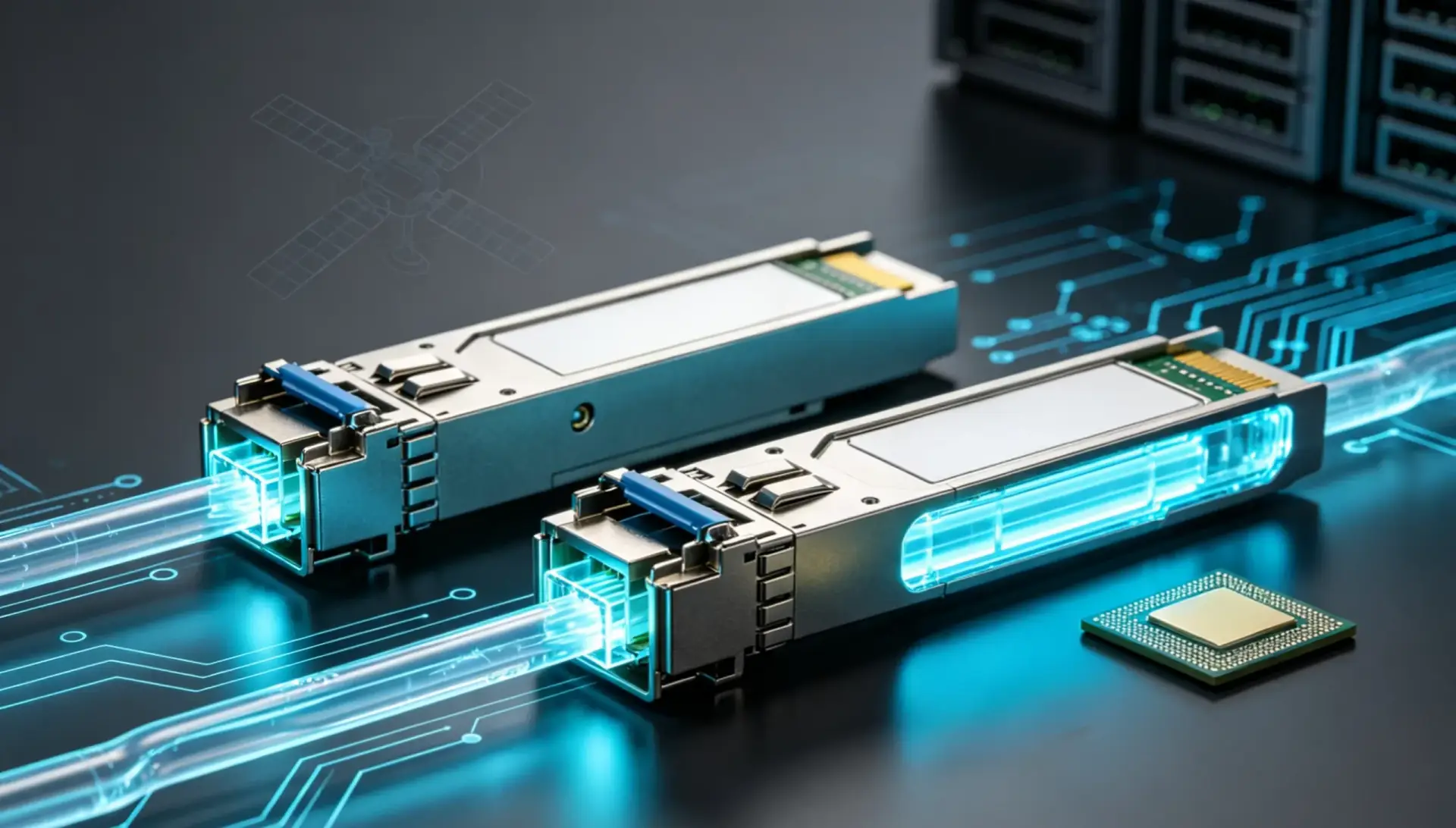
Before selecting an EMS partner, engineers need to classify the module by application. A data center link, a long-reach laser module, and a satellite communication T/R module may all involve optical transmission, but they create different manufacturing risks.
For 400G and 800G projects, data rate affects connector layout, power budget, signal routing, thermal control, and inspection planning. DEEPETCH’s transceiver catalog includes OSFP-800G-2xSR4 and QSFPDD-800G-SR8 references. These modules operate at 3.3V with power consumption of ≤14W, use 850nm wavelength transmission, VCSEL+PIN components, and MPO/APC connector structures, with listed reach of 60m on OM3 or 100m on OM4 fibers.
This data helps procurement engineers avoid vague requests. Instead of asking whether a supplier can support 800G, ask whether it can review optical connector type, signal path, heat load, component matching, and test records together.
Reach changes the packaging logic. Short-reach modules often focus on connector fit, electrical continuity, and stable assembly. Long-reach designs need more attention to laser package protection, detector alignment, sealing, and temperature behavior. For a laser-based Optical Module, package selection should be discussed before the EMS plan is frozen.
Custom assemblies for aerospace, satellite communication, radar products, and 6G communication hardware may require different packaging materials, board layouts, and environmental review. DEEPETCH provides TR transceiver chips and TR transceiver modules for satellite communication and radar products, so optical, RF, and PCBA requirements can be reviewed together at an early stage.
A module can pass a simple electrical check and still fail later because of heat concentration, signal loss, package leakage, or weak process transfer. The EMS plan should match the real field condition, not only the drawing.
Signal integrity depends on controlled routing, short transitions, stable package structure, and substrate capability. In high-speed optical transceiver EMS, the substrate is part of the signal path. DSP chips, driver ICs, and control chips need a routing structure that can support dense interconnection near the optical signal chain.
Thermal design is now a purchasing checkpoint for AI computing and supercomputing centers. Air cooling may not be enough for dense racks and high-speed optical links. DEEPETCH provides 10G to 800G immersion liquid-cooled transceivers and Active Optical Cables for liquid-cooled data centers.
One useful reference is OSFP-400G-SR4-YL. It is listed with 400Gbps data rate, 3.3V supply voltage, ≤8W power consumption, 850nm VCSEL+PIN components, MPO-12/APC connector, and 0°C to 60°C case temperature range. This gives engineers a concrete baseline when comparing standard builds with immersion liquid-cooled transceivers.
A working sample is not enough. Engineers should check whether reliability testing follows real risk points, such as delamination, open/short failure, solder heat resistance, humidity stress, and resistance shift. DEEPETCH’s IC substrate reliability test data includes JEDEC-based items such as MSL3 preconditioning, HTST, THB, TCT, BHAST, and PCT. For example, TCT uses -55°C to 125°C cycling for 1000 cycles, while BHAST uses 130°C, 85%RH, 10V, and 168 hours.
For procurement qualification, engineers can also request documents connected with DEEPETCH’s listed management systems, including ISO 9001, IATF 16949, ISO 14001, ISO 17025, ESD control, and ISO/IEC 27001. This matters because a custom Optical Module project depends not only on one successful prototype, but also on stable process control when the project moves into repeat orders.
After the module type is clear, engineers can review the package and substrate technologies behind the product. This step connects the Optical Module type with the actual manufacturing path.
The Butterfly package is a practical fit for laser-based optical communication, LiDAR, microwave electronics, satellite communication, and radar-related modules. A butterfly package configuration can support ceramic protection, optical access, signal transmission, and heat transfer in one structure.
For long-reach telecom links or satellite T/R module projects, engineers should confirm package layout, pin design, sealing logic, optical window needs, and thermal path before sample production. This helps avoid late-stage package redesign after the circuit has already been approved.
The FCBGA Substrate is relevant when the project involves advanced chip packaging requirements. DEEPETCH describes FCBGA Substrate with Build-up Film Lamination and SAP process, supporting applications such as HPC, GPU, CPU, FPGA, AI computing, 5G/6G hardware, high-speed switches, routers, and optical modules.
For high-speed routing, FCBGA substrate for optical modules can support dense interconnection around DSP, driver ICs, and control chips. Engineers should review multilayer build-up structure, micro via formation, and substrate process control before approving mass production.
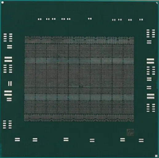
Many failures come from early assumptions that were never checked. The first pitfall is treating the substrate as a passive background component. At 400G and 800G speeds, weak matching between fine interconnection, multilayer build-up, and package layout can damage signal integrity.
The second pitfall is poor traceability. In advanced custom assemblies, a single faulty component or hidden process drift can affect a high-value T/R module. DEEPETCH’s Smart Plant full-process traceability covers material preparation, laser pretreatment, laser via, AOI with E-Mapping, pressing, solder resist, ENEPIG, bump inspection, O/S test with E-Mapping, FVI, sorting, packing, and ship-out. This process trail helps engineers locate the source of defects instead of only replacing failed units after shipment.
The third pitfall is weak failure analysis. For advanced chip and package projects, DEEPETCH’s product analysis services include Probe Test, IV Curve, TDR, high power microscope, Scanning Acoustic Tomography, 2D X-ray, 3D X-ray, Decap, Crater, Ion-milling, Focussed Ion Beam, Cross Section, Scanning Electron Microscope, Energy Dispersive X-Ray Spectrometry, Transmission Electron Microscope, and Optical Beam Induced Resistance Change. These tools help identify solder voids, cracks, delamination, routing defects, and package-level abnormality before the same issue repeats in production.
Custom EMS should connect design review with actual manufacturing. A supplier should help identify where signal, heat, package, substrate, or reliability risks may appear.
Define application, speed, form factor, link distance, operating environment, sample quantity, and inspection items. This avoids choosing the wrong package or substrate route at the start.
Laser devices, long-reach links, LiDAR, satellite communication, and radar assemblies may point toward butterfly packaging. Dense chip packaging, AI computing hardware, 5G/6G network equipment, and high-speed electrical routing may point toward FCBGA Substrate. Some projects may need both.
DEEPETCH’s IDM customization process includes requirement communication, design optimization, sample production, quality control, production arrangement, customer service, and after-sales support. For one Optical Module project, testing may focus on signal transmission. For another, it may focus on thermal stress, sealing, connector fit, substrate reliability, or board-level inspection.
Service should be planned before production. Technical support, customer feedback processing, reliability review, traceability data, and continuous improvement help reduce repeated sample revisions and unstable repeat orders.
Before sharing your schematic with an EMS provider, define these items clearly.
| Checklist Item | What to Confirm |
|---|---|
| Form Factor and Speed | OSFP, QSFP-DD, QSFP112, QSFP56, 400G, 800G, or custom assembly |
| Optical Reach | Short-reach multimode, long-reach laser architecture, or special link design |
| Thermal Limit | Standard cooling or immersion liquid cooling requirements |
| Package Need | Standard assembly, butterfly package configuration, or other ceramic package path |
| Substrate Need | Standard board, FCBGA substrate, or high-density build-up routing |
| Reliability Tests | MSL, TCT, THB, BHAST, PCT, solderability, and solder heat resistance if required |
| Failure Analysis | X-ray, SEM, TDR, SAT, FIB, cross section, or other product analysis needs |
| Field Use | Data center, AI computing, satellite communication, radar, LiDAR, or aerospace assembly |
| After-Sales Data | Test records, failure screening, replacement logic, and feedback loop |
If your project has unclear package, substrate, TR module, reliability test, failure analysis, or liquid cooling requirements, send the application background, target environment, sample schedule, and expected inspection items through DEEPETCH’s contact channel. A clear technical file helps both sides reduce wrong material selection, weak test coverage, and repeated sample revisions.
Q: Which Optical Module projects are more suitable for a butterfly package configuration?
A: A butterfly package configuration is more suitable for laser-based modules, long-reach optical communication, LiDAR, satellite communication T/R modules, and radar-related assemblies where sealing, thermal path, and signal stability need to be reviewed together.
Q: Why does FCBGA Substrate matter in high-speed optical transceiver EMS?
A: FCBGA Substrate supports dense chip packaging and high-speed interconnection. It is useful when the project includes DSP chips, driver ICs, AI computing hardware, 5G/6G systems, high-speed switches, routers, or advanced optical modules.
Q: What quality documents should engineers ask for before starting a custom Optical Module EMS project?
A: Engineers should ask for form factor data, power and thermal limits, package and substrate specifications, reliability test plans, inspection flow, traceability method, failure analysis options, and after-sales feedback procedures. This gives both teams a clearer path from sample build to stable production.

The DE-CW-1310 DFB EPI wafer, a high-performance epitaxial structure designed for distributed feedback (DFB) lasers operating at 1310 nm....

Ceramic thin-filmvacuum sensor Optical gas massflowmeter Liquid mass flowmeter Force sensor MEMS...

Photoelectric sensing chip Light source chips Optical transmission and modulationchips Optical detection and receptionchips...

Using a“Detach Core”which has two-layers carrier foil structure on the surface as a core, and forming...

Tenting process is a kind of subtractive process, the process as follows: Laminating photosensitive film...

Modified Semi-Added Process abbreviated as mSAP, which can be used on the core or build-up layers, pattern...

Semi-Added Process abbreviated as SAP, using on the build-up-layer pattern forming as follow:First depositing...

The product generally adopts the pressing lamination process of semi-curing sheets , and line formation...

The products generally adopt the Build-up Film Lamination process, and the circuit formation uses the...
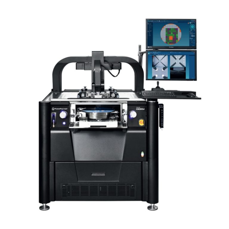
Equipment features: 1. Non-destructive precision testing Micrometer-level probe contact technology...