
Complex PCBA projects rarely fail because of one big mistake. More often, the trouble comes from small design choices that look fine on a screen but behave badly on the production line. A high-speed trace is routed too close to a noisy area. A thermal pad looks large enough, but solder flow is not stable. A connector fits the drawing, yet rework becomes painful once the housing is added. DFM, short for Design for Manufacturing, helps you catch these problems before your EMS project turns into a long cycle of redesign, delay, and cost pressure.

A prototype can pass a lab test and still be hard to build in volume. That is a common headache in aerospace circuits, satellite communication boards, drone control electronics, and 6G communication hardware. In early samples, engineers can hand-adjust parts, add jump wires, or spend more time on inspection. EMS production does not work that way. It needs repeatable assembly, clear process limits, and stable yield.
This is where DFM becomes practical. It does not replace engineering design. It simply asks a tougher question: can this board be built again and again without hidden risk?
For high-frequency PCBA design, DFM should start with layout review. Trace width, spacing, impedance, ground return, via structure, and copper balance all need to match the real process window. In 6G TR module design, even a small layout issue can raise trace resistance or bring extra capacitance. That may not be obvious in a basic continuity test, but it can show up later as signal loss, timing drift, or heat.
If your board uses fine-pitch components, dense routing, or high-speed transceiver circuits, the review should also cover solder mask clearance, pad size, via-in-pad filling, stencil opening, and inspection access. These details sound boring, but they decide whether production moves smoothly.
DFM lowers risk because it connects design intent with production limits. In a custom EMS project, you are not only buying assembly. You are buying the ability to move from schematic, PCB layout, sourcing, trial build, testing, and batch production without losing control between steps.
For buyers working on PCBA design and manufacturing, the biggest value is not just a cheaper board. It is fewer surprises after the first production lot. That matters when the product is used in aviation electronics, satellite communication systems, AI computing equipment, or 6G communication devices.
A proper DFM review checks whether your Gerber files, BOM, assembly drawing, test points, and mechanical files tell the same story. If the board outline, connector height, heat sink space, and cable route are not aligned, EMS production will slow down fast.
For example, a drone flight control PCBA may need compact routing, stable power delivery, and light weight. But if test points are buried under a shield can, production testing becomes slow. If the thermal path depends on a screw boss that has poor contact, field temperature may rise. DFM catches this before tooling, fixture design, and material purchase lock the project in.
Substrate choice is no longer just a material question. It affects signal speed, thermal behavior, package density, and long-term reliability. In high-speed electronic manufacturing, especially for 6G communication and advanced packaging, the board or package substrate has to support dense lines without causing signal loss.
That is why buyers should review substrate decisions during DFM, not after failure analysis. Once the stack-up is fixed and impedance is calculated, late material changes become costly.
The ABF substrate (epoxy resin deposited film) is a useful option for high-density interconnect and advanced packaging projects. It supports fine circuit layouts, high flatness, and strong dimensional control, which are important when your design needs compact routing and stable high-frequency signal paths.
For complex EMS production, this matters in plain terms: if the substrate cannot hold line spacing, via accuracy, or thermal stability, the best assembly line still cannot save the design. A good DFM process checks whether the selected substrate matches the target signal rate, heat load, layer count, and package structure before production starts.
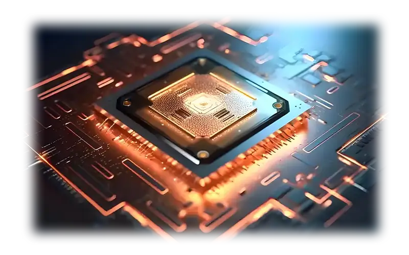
Before sending a complex board to EMS production, the design should be reviewed from both engineering and factory angles. A board may look clean in CAD, but the factory needs enough room for solder printing, placement, reflow, AOI, X-ray, ICT, functional testing, and rework. If one step is ignored, the whole project may slow down.
DEEPETCH works around semiconductor solutions, high-speed optical modules, liquid cooling solutions, high-speed cables, and AOC products, with OEM/ODM/JDM service experience for demanding communication applications. You can learn more through the DEEPETCH homepage , especially if your project sits near data center, AI computing, supercomputing, cloud computing, or 6G hardware.
A practical DFM checklist should include:
One small point from real production: test points often get treated as an afterthought. Then the factory has to build awkward probes or do manual testing. That is not a serious problem for five samples, but it becomes annoying and expensive at 500 units.
6G communication equipment, satellite boards, and aerospace circuit design all share a similar problem: the working environment is not kind. High frequency, compact structure, heat, vibration, and long service time make normal consumer-grade design habits risky.
A professional EMS flow should start with DFM, then move into DFT, sourcing review, prototype build, reliability testing, and controlled batch production. The order matters. If DFM is skipped, testing may only confirm that the design is hard to build.
For satellite communication circuit design, DFM should review impedance control, power stability, grounding, shielding, and heat transfer. For drone circuit design, it should also check vibration resistance, connector locking, board weight, and repair access. For 6G transceiver TR projects, routing density and material choice become even more sensitive because signal paths are shorter, faster, and less forgiving.
DEEPETCH has public information around IDM-related semiconductor capability, chips and stocked parts through chips in stock and company background through company overview. For buyers, this kind of structure is helpful because EMS risk is not only about assembly. It is also about component access, substrate choice, engineering feedback, and whether the supplier can discuss technical tradeoffs early.
The best time is before the PCB layout is frozen. The second-best time is before the first prototype order. Waiting until mass production is a bit late, though still better than doing nothing. Early DFM review can reduce redesign rounds and give your team a cleaner path from sample to production.
If your project involves PCBA design and manufacturing for aerospace, 6G communication, satellite hardware, or custom electronic manufacturing, you should send the EMS team more than Gerber files. Share the real use case, power range, thermal limit, signal rate, target quantity, inspection needs, and any parts that cannot be changed.
A useful DFM review should end with clear decisions. Which pads must change? Which parts need alternates? Which vias need filling? Which test points must move? Which substrate is acceptable? Which tolerance is too tight for normal production?
That is how DFM turns from a checklist into production insurance. It helps you avoid a painful situation where the board works once but cannot be built steadily. For complex EMS projects, that difference is everything. If you need to discuss a custom PCBA or semiconductor-related production plan, the DEEPETCH contact page is the most direct next step.
Q1: What Is DFM in PCBA Manufacturing?
A: DFM means Design for Manufacturing. It reviews whether your PCBA design can be built reliably in real EMS production, not just whether it works as a prototype.
Q2: Why Is DFM Important for 6G TR Module Projects?
A: 6G TR module projects involve high-frequency routing, dense layout, thermal load, and strict signal control. DFM helps reduce layout, soldering, material, and testing risks before production.
Q3: Does ABF Substrate Help Complex PCBA and Packaging Designs?
A: Yes. ABF substrate supports fine lines, high-density interconnect, and advanced packaging needs, which can help compact high-speed designs when the stack-up and process are reviewed early.
Q4: When Should a Buyer Start DFM Review?
A: Start before the PCB layout is frozen. Early review gives your team more room to adjust routing, test points, BOM choices, thermal design, and substrate selection.
Q5: Can DFM Reduce EMS Cost?
A: Yes, but not only by lowering unit price. DFM reduces hidden cost from redesign, scrap, slow testing, poor yield, delayed delivery, and field failure risk.

The DE-CW-1310 DFB EPI wafer, a high-performance epitaxial structure designed for distributed feedback (DFB) lasers operating at 1310 nm....

Ceramic thin-filmvacuum sensor Optical gas massflowmeter Liquid mass flowmeter Force sensor MEMS...

Photoelectric sensing chip Light source chips Optical transmission and modulationchips Optical detection and receptionchips...

Using a“Detach Core”which has two-layers carrier foil structure on the surface as a core, and forming...

Tenting process is a kind of subtractive process, the process as follows: Laminating photosensitive film...

Modified Semi-Added Process abbreviated as mSAP, which can be used on the core or build-up layers, pattern...

Semi-Added Process abbreviated as SAP, using on the build-up-layer pattern forming as follow:First depositing...

The product generally adopts the pressing lamination process of semi-curing sheets , and line formation...

The products generally adopt the Build-up Film Lamination process, and the circuit formation uses the...
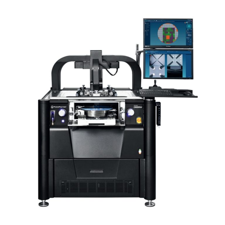
Equipment features: 1. Non-destructive precision testing Micrometer-level probe contact technology...