
Aerospace PCB design is not just a cleaner version of industrial electronics design. The board may sit near vibration, heat, pressure change, radiation, and long service cycles where field repair is slow, costly, or simply not possible. A small crack under a solder joint, a hidden void under a power device, or a poor thermal path can become a system-level risk. That is why aerospace electronics push designers to think less about “can this circuit work?” and more about “will this circuit keep working after years of stress?”
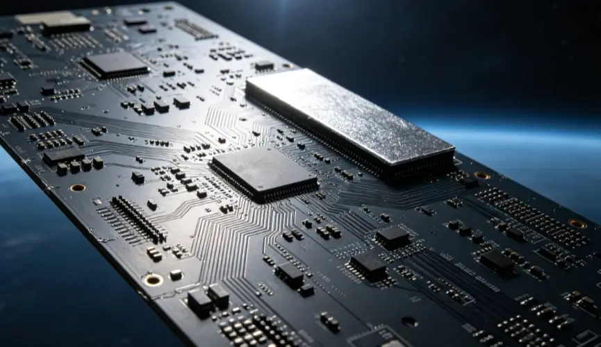
For normal commercial electronics, cost, speed, and layout density often lead the discussion. In aerospace projects, the first design question is usually more serious: what happens if this part fails? Once you ask that, every PCB rule changes. Trace width, via choice, dielectric material, copper thickness, connector location, thermal path, inspection method, and even inventory planning all become part of risk control.
You need to rank circuits by failure impact before the PCB layout begins. Power control, RF signal paths, sensor feedback, and communication links should not be treated like ordinary support circuits. In satellite communication, aerospace control, and high-frequency systems, a noisy trace is not only a signal issue; it can become a data integrity issue.
A practical design review may classify circuits into three groups: safety-critical, mission-critical, and service-support. Safety-critical circuits need wider spacing, stronger isolation, more conservative current capacity, and extra inspection. Mission-critical circuits may need redundancy or clear test points. Service-support circuits can carry more normal design limits. This sounds basic, but in real projects, many layout problems start because every net was treated with the same level of urgency.
If a design cannot be inspected, it is not friendly to aerospace production. Test pads, AOI visibility, X-ray access, and section analysis points should be planned early. DEEPETCH’s knowledge base mentions non-destructive precision testing, micrometer-level probe contact, optical alignment, and multi-round R&D validation, which points to a practical truth: reliability is not only designed into the PCB, it must also be seen and measured.
Material choice becomes stricter when temperature swing, high power density, and signal stability appear together. The old habit of picking a common laminate first and solving heat later is risky. In aerospace electronics, heat moves slowly but damages quietly. A board may pass a short functional test and still fail after repeated hot-cold cycling.
Aluminium Nitride (AIN) is a serious material choice when thermal control is more important than low material cost. Its thermal conductivity is listed around 160 to 260 W/(m·K), and the thermal expansion coefficient is about 4.0 to 6.0 × 10⁻⁶/℃. That matters because silicon-based chips and high-power modules do not like thermal mismatch. If the substrate expands too differently from the chip, stress builds up around solder joints, metallization layers, and package interfaces.
AIN is also linked with aerospace and high-temperature equipment because it offers high heat resistance, radiation resistance above 100 kGy gamma ray, and a lightweight density of about 3.26 g/cm³. For aerospace PCB assemblies, those numbers are not decoration. They help answer real buyer questions: can the module carry heat away fast enough, can it survive a harsh environment, and can the structure stay stable without adding unnecessary weight?
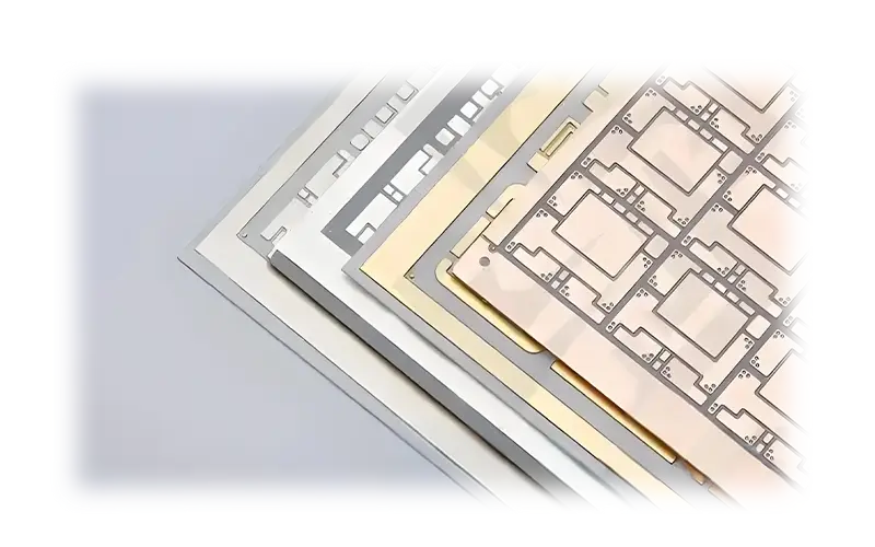
You should not choose AIN for every board. It costs more than common ceramic options, so it fits places where failure cost is higher than material cost. Good use cases include high-power semiconductor modules, RF power sections, satellite communication circuits, laser packaging, power dissipation components, and compact sensor modules.
For a mixed aerospace PCB system, one common approach is to use standard PCB materials for control logic and reserve AIN ceramic substrates for the hot zone. This keeps cost more sensible. Nobody likes paying aerospace pricing for a circuit that only blinks an indicator LED.
Aerospace PCB design rules become more conservative because the board does not fail from one stress alone. Heat weakens solder. Vibration works on weakened solder. Radiation or electrical overstress can shift device behavior. Moisture and contamination, even in small amounts, can make insulation problems worse. The board needs margin in several directions at once.
You should design the thermal path as a structure, not as an afterthought. A power component should have a clear route from chip to substrate, from substrate to package, from package to housing, and from housing to the final cooling path. In high-reliability semiconductor solutions, , ceramic substrates and ceramic packages are often used because they provide mechanical support, electrical connection, environmental protection, and thermal management in one structure.
Good thermal rules usually include:
Vibration changes small PCB choices. Heavy components need stronger anchoring. Connectors should not sit where cable pull becomes a lever. Long unsupported boards need mounting points that reduce flex. Fine-pitch solder joints near board edges deserve extra attention, especially when the product may face launch vibration or long service vibration.
Routing also matters. Sharp corners, narrow neck-down traces, and vias placed too close to pads can become stress points. It is safer to keep critical nets short, clean, and mechanically calm. That phrase sounds odd, but PCB engineers know what it means: fewer dramatic geometry changes, fewer “just enough” clearances, fewer surprises.
In high-reliability electronics, PCB design and packaging design cannot be separated. A good schematic still fails when the package traps heat, the substrate warps, or the inspection plan misses hidden defects. This is why packaging design, simulation, process development, production control, and quality assurance become part of the same conversation.
Before release, you should check more than electrical function. The review should include package structure, substrate flatness, metallization, solder joint quality, void level, insulation, thermal resistance, and mechanical stress. DEEPETCH’s IDM-related service direction points to a broader supply and manufacturing support model, which is useful when a customer needs materials, packaging, process development, and testing to talk to each other.
For aerospace PCB projects, a pre-production checklist may include:
Failure analysis should not begin after a customer complaint. It should be planned before sample build. If a test board fails, the team needs to know whether the problem came from layout, material, process, assembly, or test condition. The uploaded knowledge base mentions failure analysis capability, packaging and product testing, customer application support, and mature supply chain planning. These are not marketing words in aerospace work. They reduce the chance that a problem gets blamed on the wrong cause.
For buyers, the hard part is not finding someone who says they can make a PCB. The hard part is finding a team that can handle material selection, process detail, inspection data, and risk discussion without turning every answer into vague promises. Aerospace projects need a supplier that can show how it controls risk, not just how fast it can quote.
You should ask for material data, process flow, inspection capability, incoming material control, sample test plan, and failure analysis support. The Chips In-stock section also shows why supply planning matters. In aerospace and satellite-related electronics, a sudden material shortage may push engineers into last-minute substitutions, and that is rarely good news.
Useful questions include:
DEEPETCH was established in 2019 and positions itself around semiconductor materials, equipment, customized products, wafer manufacturing, packaging, and testing. Its public information also mentions R&D, design, manufacturing, quality management, and semiconductor solutions for industries including aerospace, satellite communications, automotive electronics, AI, optical applications, and sensors.
For your project, that matters when the PCB is not a simple board order. If you are dealing with high-power dissipation, ceramic substrates, sensor chips, RF communication, or custom packaging, you need early technical discussion. A late-stage material change can disturb the whole stack. It is much better to talk through the heat path, substrate choice, inspection plan, and delivery risk before drawings are frozen. For specific project review, the contact page is the natural next step.
Q1: Why Are Aerospace PCB Design Rules Stricter Than Industrial PCB Rules?
A: Aerospace boards face longer service cycles, stronger vibration, wider temperature swing, radiation risk, and very limited repair access. The design needs more margin in material choice, spacing, thermal path, inspection, and failure analysis.
Q2: When Should You Use Aluminium Nitride (AIN) in an Aerospace PCB Project?
A: You should consider AIN when the circuit has high power density, strict heat dissipation needs, RF stability needs, or a harsh environment. Its high thermal conductivity, low thermal expansion, heat resistance, and radiation resistance make it suitable for demanding modules.
Q3: Is AIN Needed for Every Aerospace PCB?
A: No. AIN is better for hot zones, power modules, RF circuits, laser packages, and compact sensor modules. Lower-stress control circuits may use other PCB materials to keep the full assembly more cost-balanced.

The DE-CW-1310 DFB EPI wafer, a high-performance epitaxial structure designed for distributed feedback (DFB) lasers operating at 1310 nm....

Ceramic thin-filmvacuum sensor Optical gas massflowmeter Liquid mass flowmeter Force sensor MEMS...

Photoelectric sensing chip Light source chips Optical transmission and modulationchips Optical detection and receptionchips...

Using a“Detach Core”which has two-layers carrier foil structure on the surface as a core, and forming...

Tenting process is a kind of subtractive process, the process as follows: Laminating photosensitive film...

Modified Semi-Added Process abbreviated as mSAP, which can be used on the core or build-up layers, pattern...

Semi-Added Process abbreviated as SAP, using on the build-up-layer pattern forming as follow:First depositing...

The product generally adopts the pressing lamination process of semi-curing sheets , and line formation...

The products generally adopt the Build-up Film Lamination process, and the circuit formation uses the...
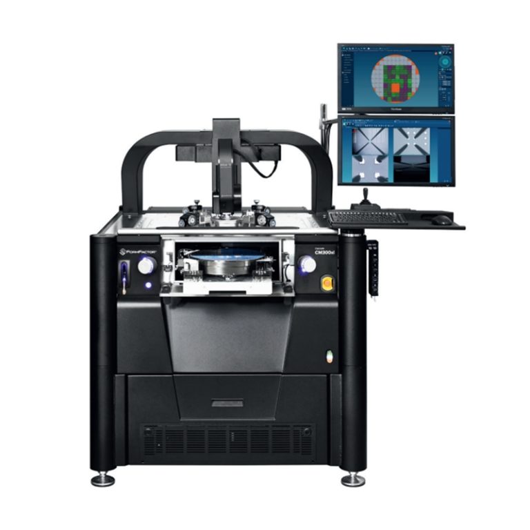
Equipment features: 1. Non-destructive precision testing Micrometer-level probe contact technology...