
Aerospace circuit design is not only a fight for smaller size or faster data speed. The real fight is between clean signal behavior and long-term survival in a rough environment. A satellite communication board, a radar front-end module, or a UAV control circuit may pass normal bench testing, yet still show phase drift, timing error, gain shift, or weak link stability after vibration, vacuum exposure, radiation stress, and thermal cycling.
For buyers, this means one thing: the supplier cannot treat aerospace electronics like common industrial PCBA work. You need the right material, the right package, the right substrate, and a process flow that can catch hidden failure points before the product goes into a satellite, aircraft, radar unit, or high-altitude platform.

Signal integrity wants short paths, low loss, stable impedance, tight grounding, and repeatable interconnection. Radiation tolerance asks for material stability, drift control, shielding logic, and long-life package behavior. These two goals often compete inside the same small circuit space, and that is where many aerospace failures begin.
In satellite communication and radar hardware, signal paths are not forgiving. A small via transition, bond wire, connector pad, or package escape route can create reflection, phase error, or insertion loss. In a TR transceiver module, that may affect gain balance, beam direction, receiver sensitivity, or radar image quality.
This is why aerospace circuit design cannot rely only on a neat schematic. The chip, package, substrate, connector, and module layout must be reviewed as one signal chain.
Radiation damage does not always break a device at once. More often, it slowly changes leakage current, threshold behavior, noise floor, gain stability, and timing response. Total Ionizing Dose (TID) can cause gradual material and device degradation, while Single Event Effects (SEE) may trigger sudden abnormal states in high-altitude or orbital conditions.
For aerospace buyers, the key question is not “Does the circuit work today?” The better question is “How does the circuit behave after stress?”
Thermal cycling and launch vibration bring another layer of trouble. Different materials expand at different rates. Solder joints, substrate layers, package cavities, metal lids, and board interfaces all move a little. That small movement can create cracks, contact resistance change, warpage, or impedance shift.
It sounds like a boring mechanical detail, but in a high-frequency radar or satellite communication module, that detail can decide whether the signal stays clean.
Material selection should start from the signal path, not from a generic parts list. If your design needs high-frequency reception, optical communication, fast response, or low-noise behavior, the semiconductor material becomes part of the system-level reliability plan.
DEEPETCH works across semiconductor materials, IC packaging substrates, sensor chips, equipment, chip supply support, and custom manufacturing support. The company has experience in 400G/800G optical module mass production and 1.6T optical module development, while also covering FCBGA/FCCSP substrates, MEMS and photoelectric sensing chips, packaging design, testing, and customized product support. For aerospace communication buyers, this mix is useful because a real project often needs more than one product category.
Indium phosphide (InP) is a strong fit for aerospace communication hardware where high-frequency behavior, photoelectric conversion, and weak signal reception matter. InP is often used in optical communication devices, laser devices, photodetectors, and high-frequency electronic devices.
For satellite communication payloads, InP can support receiver-side and optoelectronic designs where fast response and sensitivity are more valuable than simple low-cost sourcing. In radar and advanced communication links, it also helps reduce the gap between RF performance and optical signal processing.
DEEPETCH provides TR transceiver chips and TR transceiver modules for satellite communication and radar products. These modules are not simple add-on parts. They handle transmit and receive paths, phase control, gain control, signal conditioning, and electromagnetic behavior in a compact space.
For your project, this matters because the TR module is close to the “front door” of the signal. If heat, noise, shielding, or grounding is not handled well here, the rest of the system has to fight a problem that should have been solved earlier.
Aerospace communication is not always a pure RF topic now. Optical detection, laser links, optical modulation, and electrical conversion can all appear in the same hardware plan. That makes photoelectric sensing chips and optical receiving devices more relevant to satellite communication, high-speed data links, and onboard sensing systems.
A clean design should connect optical emission, modulation, detection, and electrical processing without treating each block like an isolated island.
As aerospace electronics become denser, the substrate stops being only a carrier. It becomes part of signal routing, power delivery, thermal spreading, and mechanical reliability. A poor substrate decision may not show up during early prototype testing, but it can appear later as drift, warpage, signal loss, or unstable assembly yield.
FCBGA Substrate is useful for chips that need dense interconnection, short signal paths, and stable routing. In aerospace circuits, this is not just about saving space. Fine-pitch interconnection can help reduce parasitic effects, shorten package escape routes, and support high-I/O devices used in communication, radar, and signal processing modules.
If you are building a compact payload module, every millimeter matters. Sometimes the shortest route is also the most reliable route.
ABF build-up structures support finer routing and higher interconnection density. For high-frequency aerospace circuits, the build-up process must be consistent because small changes in layer thickness, copper geometry, or via registration may change impedance and signal loss.
A buyer should not only ask whether the substrate can be produced. You should ask whether the supplier can keep the same electrical behavior from prototype to repeat production.
A large package, dense routing, and mixed materials can cause warpage after reflow or thermal cycling. Once warpage appears, the risk is not limited to poor appearance. It may affect solder joint life, contact resistance, and package-to-board reliability.
For aerospace circuit design, FCBGA Substrate selection should include heat path review, coefficient matching, layer structure, void control, and assembly process windows. It is not fancy work, but it saves a lot of trouble later.

Reliability control should begin before mass production. Waiting until final testing is too late because many aerospace failures come from early material decisions, package mismatch, moisture behavior, hidden voids, weak interfaces, or process drift.
A good prototype only proves the first design route is possible. It does not prove that the product is ready for repeat orders. For aerospace electronics, the production path should include material traceability, package inspection, impedance review, environmental stress screening, and failure analysis feedback.
For InP devices, the focus should include crystal quality, surface condition, photoelectric behavior, leakage trend, and response stability. For FCBGA-based assemblies, the focus should include layer registration, via integrity, warpage, solder joint quality, and voiding after reflow.
Beyond generic component qualification, stable aerospace production needs controls against orbital and high-altitude failure modes. For custom satellite assemblies and radar products, DEEPETCH can support early-stage material screening logic around TID degradation risk, SEE sensitivity review, and package-level stress behavior.
Vacuum compatibility also deserves attention. Materials used in satellite assemblies should go through outgassing review, while vacuum reflow needs strict voiding control so that hidden bubbles do not become weak thermal or mechanical points. By pairing product analysis services with ESD control, environmental stress screening, and microstructure inspection, aerospace assemblies based on InP and FCBGA structures can move toward a more stable production state.
Failure analysis should not be treated as a repair step after something goes wrong. It should feed back into design and manufacturing. DEEPETCH’s broader capability map includes packaging and product testing, laboratory accreditation capability, failure analysis capability, customer application support, and mature supply chain planning.
In real B2B projects, this is where many suppliers are separated. Some can ship parts. Fewer can help explain why a part failed and how to stop the same problem from coming back.
Aerospace projects usually move slowly during design review, then become urgent once the qualification path is fixed. That is why you should check technical fit, production repeatability, and supply readiness at the same time.
Start with the signal chain. If your project needs low-noise reception, fast optical response, or high-frequency behavior, InP should be reviewed early. If your project needs dense routing, high I/O, and compact package integration, FCBGA Substrate should enter the design discussion before the layout is nearly finished.
For TR transceiver chips and modules used in satellite communication and radar products, material, package, substrate, and thermal structure must be matched together.
Ask about inspection before you ask only about price. Aerospace failures often hide in voids, cracks, alignment errors, contamination, weak plating, or layer shift. Optical inspection, probe testing, X-ray inspection, aging tests, and failure analysis all help reveal problems that are hard to see from normal electrical results.
DEEPETCH’s IDM route is useful for buyers who want to connect material selection, device design, packaging, testing, and application support within one technical conversation.
Qualification is expensive, so supply stability matters. If you qualify a part and then face long lead times or unstable replacement options, the project loses time. DEEPETCH’s chips in-stock resource can help buyers check availability while planning custom materials, substrates, or module-level products.
For early evaluation, buyers can also contact the DEEPETCH technical team to discuss InP devices, FCBGA Substrate, TR transceiver chips, TR transceiver modules, and aerospace-grade screening needs.
| Checklist Item | What to Confirm |
|---|---|
| Material Route | InP suitability for frequency, sensitivity, optical response, and radiation-related drift risk |
| Package Route | FCBGA Substrate structure, ABF build-up consistency, warpage control, and heat path design |
| Module Route | TR transceiver chip and module behavior in satellite communication and radar products |
| Test Route | Probe testing, optical inspection, X-ray review, aging test, ESS, ESD control, and failure analysis |
| Production Route | Prototype-to-production consistency, traceability, supply readiness, and custom support |
Q1: Why Is Signal Integrity So Difficult in Aerospace Circuit Design?
A: Aerospace circuits often combine high frequency, dense routing, vibration, thermal cycling, radiation exposure, and limited space. A small impedance mismatch or package transition can affect phase, gain, timing, or receiver sensitivity.
Q2: Why Is Indium Phosphide InP Useful for Aerospace Communication Hardware?
A: Indium phosphide (InP) is useful for high-speed optical communication, photodetection, low-noise reception, and high-frequency devices. These features make it suitable for satellite communication payloads, advanced receivers, and optical link designs.
Q3: How Does FCBGA Substrate Support Aerospace Electronics?
A: FCBGA Substrate supports dense interconnection, shorter signal paths, fine routing, and advanced package integration. In aerospace hardware, it helps manage signal loss, thermal paths, package size, and assembly reliability.
Q4: Why Are TID, SEE, and Outgassing Checks Important?
A: TID can cause gradual device degradation, SEE can create sudden abnormal behavior, and outgassing can affect vacuum reliability. These checks help buyers judge whether a circuit is suitable for high-altitude or orbital operation.
Q5: What Should You Ask Before Choosing an Aerospace Circuit Manufacturing Partner?
A: Ask about material screening, package design, substrate capability, TR module experience, inspection flow, environmental stress screening, failure analysis, and supply continuity. These points matter more than a simple unit price in aerospace projects.

The DE-CW-1310 DFB EPI wafer, a high-performance epitaxial structure designed for distributed feedback (DFB) lasers operating at 1310 nm....

Ceramic thin-filmvacuum sensor Optical gas massflowmeter Liquid mass flowmeter Force sensor MEMS...

Photoelectric sensing chip Light source chips Optical transmission and modulationchips Optical detection and receptionchips...

Using a“Detach Core”which has two-layers carrier foil structure on the surface as a core, and forming...

Tenting process is a kind of subtractive process, the process as follows: Laminating photosensitive film...

Modified Semi-Added Process abbreviated as mSAP, which can be used on the core or build-up layers, pattern...

Semi-Added Process abbreviated as SAP, using on the build-up-layer pattern forming as follow:First depositing...

The product generally adopts the pressing lamination process of semi-curing sheets , and line formation...

The products generally adopt the Build-up Film Lamination process, and the circuit formation uses the...
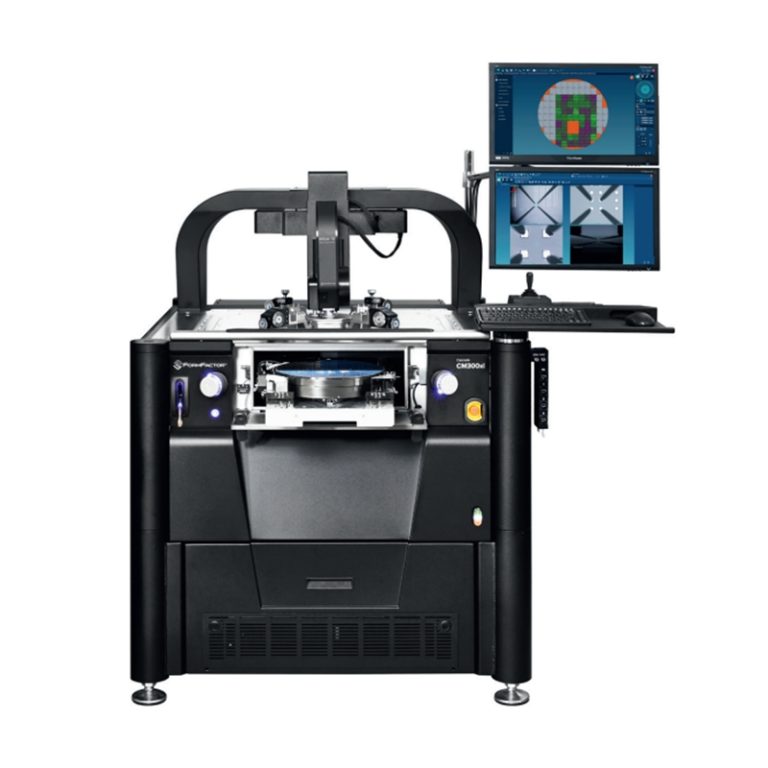
Equipment features: 1. Non-destructive precision testing Micrometer-level probe contact technology...