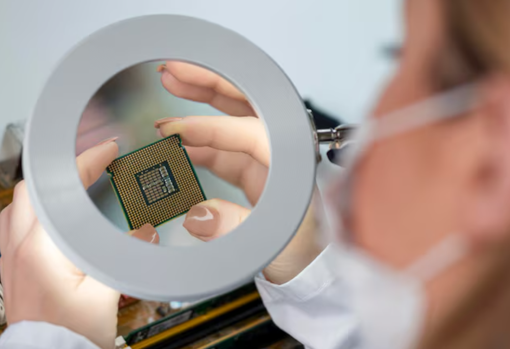
The quest to blend high linearity with extreme sensitivity in sensor chips has puzzled engineers for years. Linearity means the sensor’s output moves in step with its input, giving steady, predictable results. Sensitivity, meanwhile, is about spotting the tiniest signals. These two traits often tug in opposite directions, making designers pick one over the other based on what the job needs. But thanks to breakthroughs in chip-making, circuit tricks, and new materials, this tug-of-war is easing up. Companies like DEEPETCH are stepping in with fresh ideas to tackle this challenge. DEEPETCH, based in Shenzhen, is a high-tech outfit that handles everything from research to production. Its all-in-one approach, called the IDM model, lets it craft sensor chips tailored to specific tasks. Whether it’s for cutting-edge medical gear or tough industrial setups, DEEPETCH’s know-how delivers solutions that hit the mark.
Getting both linearity and sensitivity in one chip is tricky because they don’t play nice together in older designs. The issue comes down to physics, noise in circuits, and the stuff chips are made of.
To make a sensor super sensitive, it has to pick up the smallest changes. Random electrical junk—starts creeping in, muddling the output. On the flip side, linearity needs a clean, steady signal across a wide range, which gets tough when the sensor is stretched to detect faint inputs. Sensor chips turn things like pressure, light, or chemical changes into electrical signals, but balancing both goals is a tightrope walk.
Traditional materials, like plain silicon, can’t always keep up. They’re decent but struggle to be both super responsive and rock-solid stable. Picking the right material depends on what the sensor measures, how precise it needs to be, and how much power it can use. Some materials, like ceramics or glass, handle harsh conditions well but aren’t as quick to react as newer options like MEMS (tiny mechanical systems). Standard chip-making methods also hit walls when trying to build the complex shapes needed for top-notch sensitivity.
Dynamic range is how much signal a sensor can handle, from faint to strong. Resolution is about catching the smallest change. Boosting one often weakens the other. A sensor with a huge range might miss tiny details, like trying to hear a pin drop during a concert. Meanwhile, a sensor tuned for fine details might overload when signals get big, like a scale that’s great for weighing feathers but breaks under a heavy box.
Modern chip engineering is finding ways to ease these conflicts. From better building methods to smarter circuits, the industry is making strides toward sensors that do both jobs well.
New methods like MEMS lithography, dry etching, and 3D printing at the micro level let companies shape tiny, precise structures. Techniques like Modified Semi-Added Process (mSAP), Semi-Added Process (SAP), and maskless lithography make chips with cleaner signals and fewer errors. These tricks help sensors stay linear while picking up faint signals, thanks to tighter control over how they’re made. For example, dry etching carves out delicate parts with pinpoint accuracy, cutting down on signal fuzz.
Adding low-noise amplifiers right on the chip helps boost weak signals without garbling them. Picture a radio that picks up a faint station without static. Combining sensing parts with processing circuits, like analog-to-digital converters or filters, in one chip (called a System-on-Chip or SoC) cuts down on outside noise. This is key for jobs needing high sensitivity, like detecting a single molecule in a medical test.
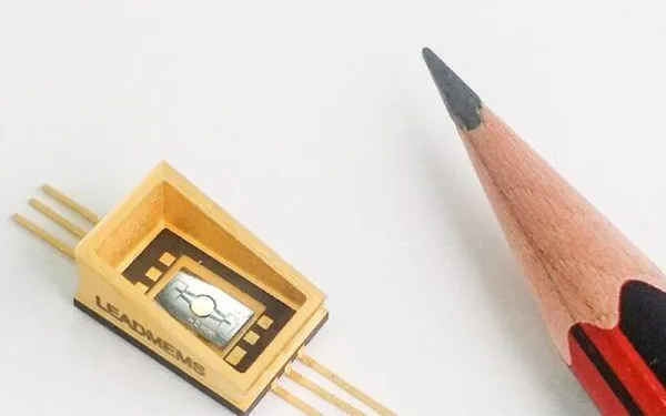
MEMS platforms make sensors that move mechanically but stay electrically solid. They’re like tiny springs that flex just right without losing their spark. Materials with low lag and good heat resistance also help. DEEPETCH, for instance, uses MEMS, ceramics, and glass micro-fusion to build sensors that hit both targets. Their years of experience with these materials make a big difference.
DEEPETCH’s Sensor Chip Series is built to solve the linearity-sensitivity puzzle with clever designs and a one-stop production system.
The series includes chips for light sensing, optical data transfer, and MEMS micro-gyroscopes, all tweaked to work as a team. Custom MEMS designs, like superlens structures, 3D-printed modules, and bistable microswitches, give tight control over how signals flow. This means better linearity and sensitivity, whether the chip is tracking motion in a car or light in a lab.
DEEPETCH’s chips shine in tough settings, from car systems to AI-powered gadgets. They’re used in phones, factory machines, medical tools, and more, proving they can handle the heat. For instance, their sensors keep working in freezing cold or scorching heat, which is critical for things like self-driving cars or heart monitors.
These chips play nice with modern setups, whether it’s a smart home device or a high-speed data collector. They keep signals accurate no matter the platform, making them a go-to for engineers juggling complex projects.
DEEPETCH’s all-in-one IDM model keeps every step of sensor-making under one roof, which speeds things up and keeps quality high.
They handle everything—design, wafer production, assembly, and testing. This cuts out middlemen and speeds up delivery. It’s like a restaurant that grows its own ingredients, cooks the meal, and serves it fresh. Their electronic manufacturing and circuit board assembly (PCBA) services ensure every chip is ready to roll.
DEEPETCH teams up with top Chinese universities and labs to explore new materials and techniques. This keeps their chips cutting-edge, with each new version better than the last. For example, testing new coatings might make a sensor tougher in humid conditions.
With designers and builders working side by side, DEEPETCH can tweak designs fast. If a test shows a glitch, they fix it on the spot, not weeks later. This teamwork keeps their chips reliable and ready for real-world challenges.
Some fields can’t compromise on either linearity or sensitivity. These sensors have to be spot-on, no matter the conditions.
Think of a wearable heart monitor or a glucose sensor inside the body. These need to catch tiny signals, like a faint electrical pulse, while staying linear across a range of readings. A chip that misreads a signal could mean a wrong diagnosis, so precision is critical.
In factories, sensors guide robotic arms or control chemical flows. They need rock-solid linearity to keep systems predictable, especially in safety-critical jobs like oil refining. A sensor that drifts could cause a shutdown or worse.
Air or water quality sensors must detect trace pollutants, like a few parts per billion, while also handling big spikes. For example, a water quality chip might need to spot tiny toxin levels in a stream but also measure heavy contamination during a spill. Both tasks demand top sensitivity and linearity.
For engineers chasing top-tier performance, DEEPETCH offers a solid track record and flexible options.
DEEPETCH’s automated production lines and strict quality checks ensure every chip works, even under stress. Their sensors pass tests in extreme heat, cold, or vibration, making them a safe bet for critical systems.
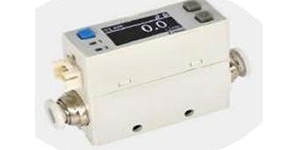
From pressure sensors using thin-film tech to flow meters based on heat transfer, DEEPETCH has a chip for every need. Their portfolio covers everything from tiny consumer gadgets to heavy-duty industrial gear.
DEEPETCH offers round-the-clock technical help, so engineers anywhere can solve problems or try new setups quickly. This is a lifesaver when deadlines are tight or a prototype needs tweaking.
Q1: Can one sensor chip really handle both high sensitivity and linearity?
A: Yes. With smart MEMS designs and advanced building methods like dry etching or mSAP, it’s possible to nail both without trade-offs.
Q2: How does the IDM model help sensor development?
A: It keeps design, production, and testing in-house, cutting delays and boosting quality.
Q3: Which fields need both high linearity and sensitivity most?
A: Medical devices, factory automation, and environmental monitoring rely on this combo for accurate results.

The DE-CW-1310 DFB EPI wafer, a high-performance epitaxial structure designed for distributed feedback (DFB) lasers operating at 1310 nm....

Ceramic thin-filmvacuum sensor Optical gas massflowmeter Liquid mass flowmeter Force sensor MEMS...

Photoelectric sensing chip Light source chips Optical transmission and modulationchips Optical detection and receptionchips...

Using a“Detach Core”which has two-layers carrier foil structure on the surface as a core, and forming...

Tenting process is a kind of subtractive process, the process as follows: Laminating photosensitive film...

Modified Semi-Added Process abbreviated as mSAP, which can be used on the core or build-up layers, pattern...

Semi-Added Process abbreviated as SAP, using on the build-up-layer pattern forming as follow:First depositing...

The product generally adopts the pressing lamination process of semi-curing sheets , and line formation...

The products generally adopt the Build-up Film Lamination process, and the circuit formation uses the...

Equipment features: 1. Non-destructive precision testing Micrometer-level probe contact technology...