In the world of chip-making, how chips are put together matters just as much as how they’re designed. Recently, one technique has been grabbing attention: CoWoS Packaging, short for Chip-on-Wafer-on-Substrate. This isn’t just a fancy name—it’s a major leap forward for creating quicker, tinier, and more dependable gadgets. DEEPETCH, a trusted name in ceramic semiconductor equipment, plays a key role in supporting precise assembly lines that meet the strict demands of CoWoS Packaging. Their tools are used in critical areas like satellites, defense tech, and top-tier data centers where mistakes aren’t an option.
Before exploring its perks, let’s break down what CoWoS Packaging does and why it’s a hot topic in the industry.
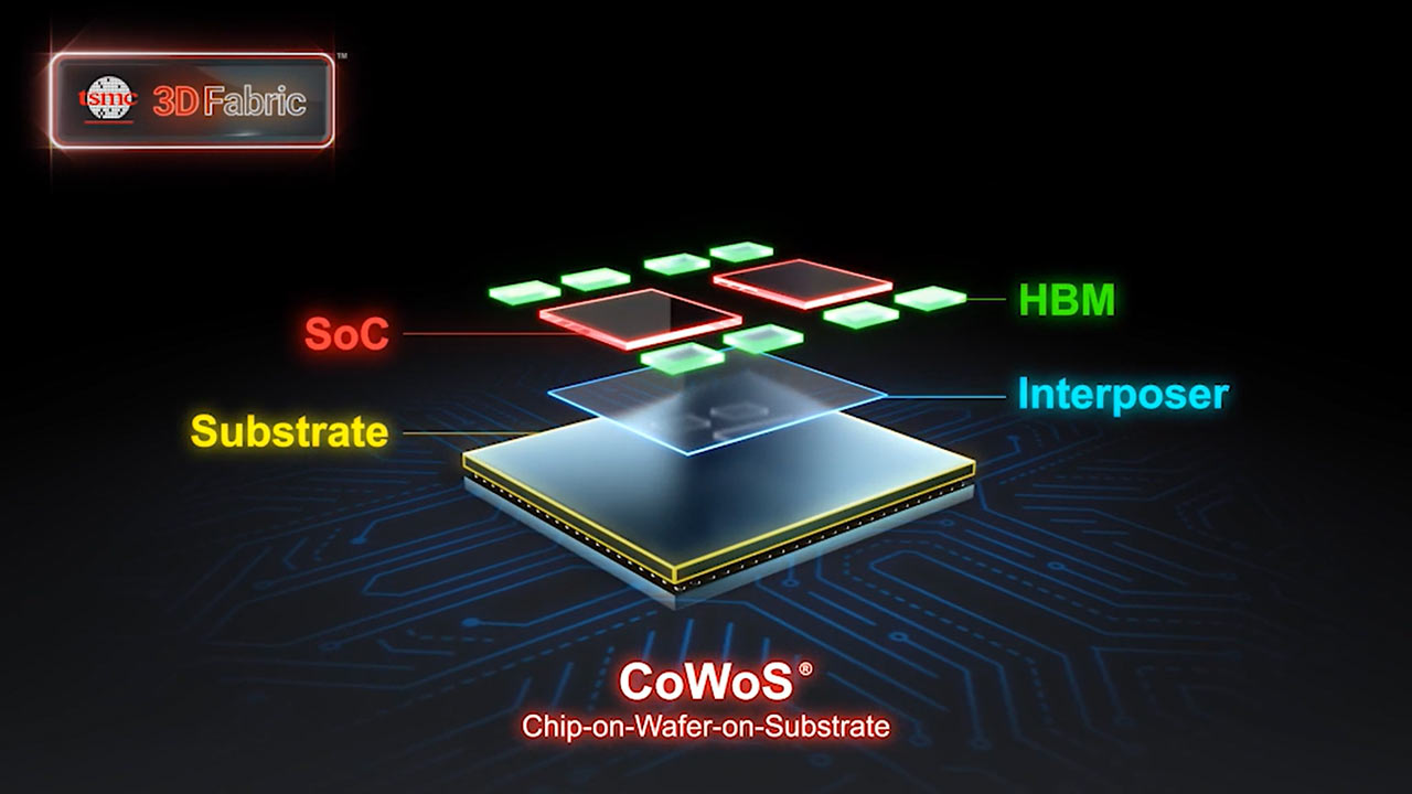
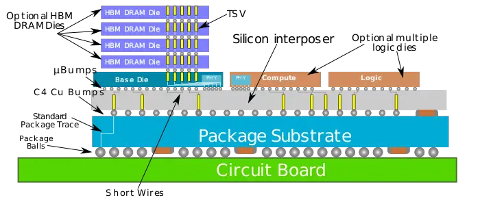
At its core, CoWoS Packaging links multiple chips using a silicon interposer. This interposer works like a speedy bridge, letting chips share data without the slowdown of long wires. Instead of placing chips far apart on a circuit board, they’re positioned close—sometimes side by side, sometimes stacked—with thousands of tiny connectors called micro-bumps.
The upside is clear: shorter paths lead to quicker data flow. Quick data flow boosts performance. It’s like having your desk next to the printer—you spend less time walking.
Compared to standard 2D packaging, CoWoS Packaging is a game-changer. In 2D setups, chips sit apart with longer connections, which can slow signals. CoWoS brings chips closer on the interposer, slashing those distances. Unlike full 3D stacking, CoWoS leaves room for heat to escape, making cooling easier.
This mix of speed and heat control makes CoWoS a top pick for high-performance processors, especially those paired with HBM (High Bandwidth Memory).
The clearest use is in AI computing. Many GPUs that power large AI models rely on CoWoS Packaging to move massive data chunks between the processor and memory in a flash. But AI isn’t the only field—networking equipment, aerospace radar, and scientific tools also use it. Any system needing top speed and reliability often turns to CoWoS.
CoWoS Packaging sounds amazing, but it only works if every piece fits perfectly. The margins for error are tiny, and a single misstep can wreck the whole package.
A typical CoWoS package might have tens of thousands of micro-bumps, each smaller than a human hair. If one is off by just a few microns, it can cause a broken circuit or a short. DEEPETCH’s pick-and-place tools tackle this issue. They use vision-guided systems to place parts with an accuracy of ±5 μm.
Picture it like threading a needle repeatedly, thousands of times, without ever missing.
Another hurdle is that materials expand when hot. In a CoWoS package, you’ve got silicon, copper, and other materials packed tightly. If they expand at different rates, stress builds. Over time, this can lead to cracks. DEEPETCH uses ceramic carriers and steady bonding techniques to keep expansion in check during assembly.
The chips in a CoWoS package can cost thousands of dollars combined. A flaw in assembly doesn’t just waste the packaging—it ruins those pricey chips too. That’s why precise tools and early defect checks are critical. Inline inspection systems catch issues before the package is sealed, saving time and money.
DEEPETCH does more than sell machines. They provide a blend of stability, adaptability, and precision for CoWoS production.
Ceramic is common in CoWoS processes because it stays stable at high heat and resists bending. DEEPETCH creates tools and carriers that hold parts securely without causing damage. This is vital for fragile dies that might crack under pressure.
Automation cuts out human mistakes. DEEPETCH’s systems adjust placement force, control bonding heat, and manage humidity levels. These small details lead to big improvements in reliability.
While CoWoS Packaging is a priority, many factories also handle other package types like CBGA or CLCC on the same line. DEEPETCH’s equipment switches between these without long pauses, letting factories adapt to shifting needs.
Picking CoWoS isn’t about following trends—it delivers real benefits in speed, heat control, and growth potential.
With memory and logic chips close together, CoWoS Packaging supports huge data transfer rates and quick responses. This is critical for systems like real-time data analysis or high-speed trading servers that can’t tolerate lag.
CoWoS helps spread heat evenly. Instead of hot spots that harm chips, the design moves heat away from key parts. This keeps performance steady over time.
As chip sizes shrink, CoWoS Packaging offers a way to add new components without a full redesign. Manufacturers can swap one die for a newer version while keeping the rest of the package.
The CoWoS journey is far from over. What we see now is just the beginning.
Soon, CoWoS packages might combine CPUs, GPUs, AI accelerators, and memory from various makers into one unit. This offers more options but demands even tighter precision.
Some factories are testing machine learning tools. These adjust placement speed, bonding time, and heat settings based on live defect data. It’s not a far-off dream—it’s already being tested in cutting-edge plants.
Researchers are exploring interposer materials and bonding compounds that can handle tougher settings, like aerospace or heavy machinery.
Q1: Why is CoWoS better than traditional 2D packaging?
A: It cuts connection lengths, boosts speed, and improves heat management.
Q2: Can CoWoS work with HBM memory?
A: Yes, it’s often used to pair HBM with high-performance processors.
Q3: What industries gain the most from CoWoS Packaging?
A: AI computing, aerospace, fast networking, and scientific research.

The DE-CW-1310 DFB EPI wafer, a high-performance epitaxial structure designed for distributed feedback (DFB) lasers operating at 1310 nm....

Ceramic thin-filmvacuum sensor Optical gas massflowmeter Liquid mass flowmeter Force sensor MEMS...

Photoelectric sensing chip Light source chips Optical transmission and modulationchips Optical detection and receptionchips...

Using a“Detach Core”which has two-layers carrier foil structure on the surface as a core, and forming...

Tenting process is a kind of subtractive process, the process as follows: Laminating photosensitive film...

Modified Semi-Added Process abbreviated as mSAP, which can be used on the core or build-up layers, pattern...

Semi-Added Process abbreviated as SAP, using on the build-up-layer pattern forming as follow:First depositing...

The product generally adopts the pressing lamination process of semi-curing sheets , and line formation...

The products generally adopt the Build-up Film Lamination process, and the circuit formation uses the...

Equipment features: 1. Non-destructive precision testing Micrometer-level probe contact technology...