Aerospace electronics usually fail from small weak points, not from one obvious mistake. A slightly long signal path, poor heat flow under a chip, mismatched expansion between package and board, or weak solder fatigue control can all turn into trouble after vibration, thermal cycling, or long service time. For aerospace PCBA design, the IC substrate is not a small packaging detail. It is the first place where signal, heat, size, and reliability meet.
Before you lock the PCB stack-up, connector position, component spacing, and assembly route, the chip package has already decided part of the system behavior. If substrate issues are ignored early, later PCBA changes become slow and costly.
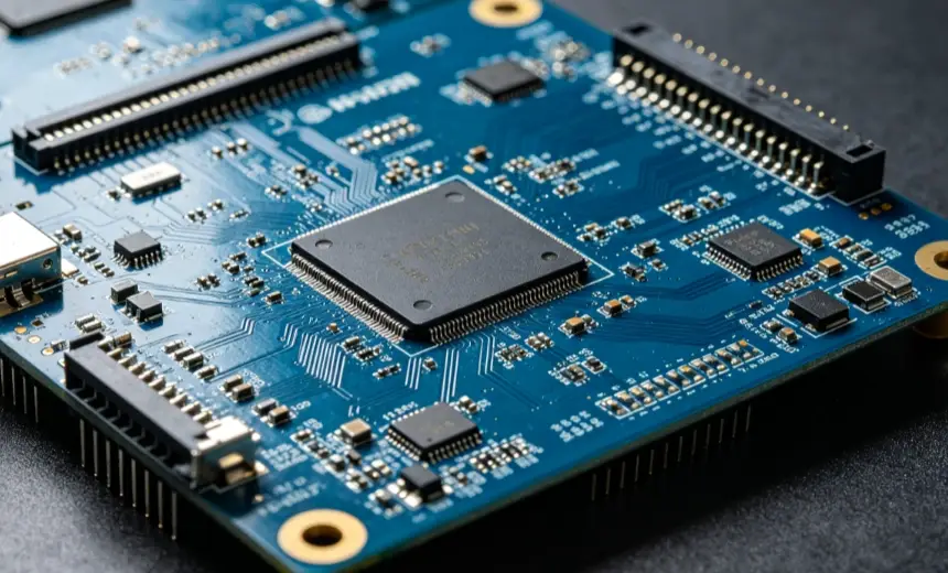
An IC substrate sits between the die and the printed circuit board. It routes signals outward, carries power and ground, and gives the chip a stable connection to the PCBA.
For aerospace electronics, this bridge must handle more than basic connection. A satellite communication board may include RF signals, digital control, power rails, timing signals, and monitoring feedback in a very compact space. If the substrate cannot support clean routing, the PCB layout may need longer traces, extra vias, and more board area. That is not ideal when the final module must fit into a small payload or UAV housing.
Heat starts at the chip junction and travels through the package, substrate, solder joints, copper layers, thermal vias, and enclosure. If the IC substrate cannot move heat fast enough, the PCB must carry the burden with larger copper areas, heavier planes, or extra heat sinks.
Aerospace products often face cold soak, sunlight exposure, shadow periods, launch vibration, or long high-load operation. Even a UAV control board can heat up fast when edge computing, RF communication, and motor control sit close together. A better substrate gives the PCBA designer more room to work.
Aerospace PCBA reliability depends on the full chain: chip, package, substrate, PCB material, soldering, coating, inspection, and testing. The substrate appears early in this chain, so a small problem there may show up later as a field failure.
When the chip, substrate, solder joint, and PCB expand at different rates, stress builds slowly. A board may pass the first electrical test, but after repeated temperature cycles, solder fatigue, micro-cracks, package warpage, or bond damage can appear.
That is why substrate selection should be reviewed together with the assembly plan. You need to check package flatness, solder joint shape, reflow profile, and material compatibility. It sounds like small work, but this is often where reliable aerospace electronics are made.
Satellite links, phased-array systems, radar boards, and future 6G communication hardware all push signal paths to higher speed and higher frequency. At this point, the substrate is part of the signal path, not just a carrier.
Semiconductor material knowledge also matters here. GaAs is known for high electron mobility and is useful in RF amplifiers, microwave devices, and satellite communication equipment. SiC is valued in high-power and high-temperature conditions. GaN fits high-frequency and high-power devices. These choices show a simple rule: chip material, IC substrate, and PCBA layout must be treated as one system.
When heat becomes a design limit, substrate material becomes a key decision. For compact aerospace electronics, you may need strong heat spreading, stable electrical behavior, and long service life. This is where Aluminium Nitride (AIN) can be useful.
In RF, sensing, control, and communication modules, heat must leave the die quickly. If heat stays near the chip, local hot spots may cause drift, noise, lower output stability, or faster aging.
For example, a compact satellite communication unit may place a power amplifier close to timing circuits and digital control ICs. You cannot always add a large heat sink because weight and space are limited. Aluminium Nitride (AIN) can help build a shorter heat path, so the board-level thermal design does not become too heavy or too crowded.
Aerospace modules usually have the same problem: every function wants the same space. RF traces need short routes. Power parts need heat paths. Digital circuits need clean return current. Mechanical teams want lower height. Test engineers still need access points.
Aluminium Nitride (AIN) is not chosen only because it sounds advanced. It makes sense when the product needs higher power density, stronger thermal behavior, and stable operation in harsh conditions. In those projects, a suitable substrate may reduce later PCBA redesign.
A good substrate choice only helps when it matches the real manufacturing process. A material table may look fine, but assembly yield, inspection access, and test coverage decide whether the design can move from prototype to production.
DFM should begin while the design is still flexible. At this stage, you can still adjust package size, pad layout, grounding, power grouping, and thermal path.
For custom PCBA, the review should ask direct questions. Can the land pattern support stable soldering? Is the pitch friendly to inspection? Will the package and PCB stack-up create warpage risk during reflow? Are there enough test points without hurting signal quality? Can the design move from a few prototypes to batch production without a full restart?
This is where DEEPETCH fits into a broader electronics manufacturing discussion. Its knowledge base covers high-speed optical modules, package design, process development, testing, sensor solutions, and OEM/ODM/JDM support. For aerospace buyers, the value is not only board assembly. It is the ability to review signal, heat, package, assembly, and validation together.
If the substrate team, PCB designer, and assembly team work separately, hidden problems appear late. A package may need a reflow profile that the board material does not like. A dense package may block inspection. A thermal pad may need void control that was not planned at the process stage.
DEEPETCH materials mention package design, simulation, package process development, packaging processing, and testing services. For aerospace PCBA, testing should not only prove that the board powers on. It should check temperature rise, signal behavior, electrical margin, and possible failure points before the product enters a costly application.
IC substrate design becomes more important when the product must be smaller, faster, hotter, and more reliable at the same time. Aerospace electronics often sits exactly in this zone.
Satellite communication electronics need stable signal transmission in a complex electromagnetic environment. The signal path from chip to substrate, from substrate to PCB, and from PCB to connector must be planned carefully.
A poor transition may create reflection, loss, or coupling. At low speed, this may be hidden. At high frequency, it appears quickly. IC substrates help by giving the chip a shorter and cleaner escape path before the signal reaches the PCB. When paired with suitable PCB material, controlled impedance routing, and good grounding, the whole module becomes easier to tune.
Modern UAVs may carry flight control, image processing, navigation, wireless links, sensor fusion, and edge computing. The board must stay light, but it still needs enough computing power and stable power delivery.
A substrate-aware PCBA design can reduce board area by supporting higher package density and better heat paths. Instead of spreading parts across a larger board just to manage routing or temperature, you can start with better package and substrate planning. The PCB design still matters, but the starting point is cleaner.
6G communication hardware will put more pressure on high-frequency design, compact modules, thermal control, and software-hardware co-design. For transceiver and TR module manufacturing, the substrate can shape the real design limit.
DEEPETCH has built experience around high-speed data transmission. Its information lists 10G to 800G transceiver series, liquid-cooling solutions, high-speed cables, active optical cables, and full-series OEM/ODM/JDM services. It also mentions 400G/800G large-scale production and ongoing 1.6T optical module R&D. The product type is not the same as aerospace PCBA, but the engineering logic overlaps: high data rate, low latency, compact structure, low power, heat control, and stable manufacturing.
For aerospace electronics, you need more than a supplier that places components on a board. You need technical review across material, package, chip supply, process, and test.
A strong project starts with risk removal. You need to know whether the substrate material is suitable, whether the package can be built repeatedly, whether key chips are available, and whether the test plan can catch common failure modes.
DEEPETCH provides resources around chips in stock, semiconductor material knowledge, IC carrier technology, and high-speed module manufacturing. These resources can support early checks before the design is locked. In aerospace projects, one delayed chip or material can slow the full prototype schedule. Early review is not fancy, but it saves time.
A prototype should prove more than basic function. It should show whether the substrate, package, PCB, assembly process, and test plan can survive the final use case.
For a satellite board, that may mean RF signal checks and temperature cycling. For a UAV controller, it may mean vibration, power stability, and heat rise during long operation. For 6G transceiver hardware, it may mean short signal paths, heat spreading, and compact assembly checks.
Through IDM-related support and broader company capability information, DEEPETCH can support buyers who need more than one-step assembly. If your project involves IC substrate selection, Aluminium Nitride (AIN), custom PCBA design, packaging review, and aerospace reliability concerns, discuss these items before the quote becomes only a unit-price conversation. For project review, you can also use the contact page.
Q1: What Is the Role of IC Substrate in Aerospace PCBA Design?
A: IC substrate connects the chip to the PCB while supporting signal routing, power delivery, heat transfer, and mechanical reliability. DEEPETCH treats it as an early design decision because it affects layout density, thermal margin, and long-term stability.
Q2: Why Is Aluminium Nitride (AIN) Useful for Aerospace Electronics?
A: Aluminium Nitride (AIN) helps move heat away from the chip faster. DEEPETCH can connect AIN selection with package design, PCBA layout, assembly review, and testing, so the material choice supports the real product.
Q3: How Does IC Substrate Affect Satellite Communication Electronics?
A: It helps shorten and clean up the signal path between the chip and PCB. DEEPETCH can support related design checks through its high-speed communication, packaging, and manufacturing knowledge.
Q4: Can IC Substrate Choices Reduce UAV PCBA Size?
A: Yes. A suitable IC substrate can support higher package density and better heat paths. DEEPETCH can help review package, substrate, PCB layout, and prototype needs together.
Q5: When Should You Discuss IC Substrate in a Custom PCBA Project?
A: You should discuss it before schematic and PCB outline are locked. DEEPETCH can review substrate, package, material risk, chip supply, DFM, and test planning early to reduce redesign risk.

The DE-CW-1310 DFB EPI wafer, a high-performance epitaxial structure designed for distributed feedback (DFB) lasers operating at 1310 nm....

Ceramic thin-filmvacuum sensor Optical gas massflowmeter Liquid mass flowmeter Force sensor MEMS...

Photoelectric sensing chip Light source chips Optical transmission and modulationchips Optical detection and receptionchips...

Using a“Detach Core”which has two-layers carrier foil structure on the surface as a core, and forming...

Tenting process is a kind of subtractive process, the process as follows: Laminating photosensitive film...

Modified Semi-Added Process abbreviated as mSAP, which can be used on the core or build-up layers, pattern...

Semi-Added Process abbreviated as SAP, using on the build-up-layer pattern forming as follow:First depositing...

The product generally adopts the pressing lamination process of semi-curing sheets , and line formation...

The products generally adopt the Build-up Film Lamination process, and the circuit formation uses the...

Equipment features: 1. Non-destructive precision testing Micrometer-level probe contact technology...