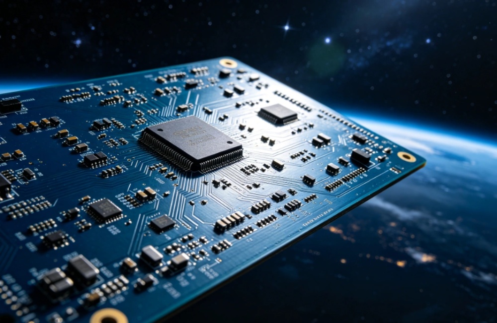
The aerospace field changes quickly as 2026 approaches. Low-earth orbit satellite groups grow fast, and 6G systems prepare to launch. The equipment inside these spacecraft encounters harsh settings that typical industrial devices cannot survive for long. If you design for important tasks, you understand that one tiny break or a bit of gas release can ruin a costly project. In this area, you must shift from regular production methods to a focused process where basic quality leads to hardware failure.
As someone with knowledge in semiconductors, I have seen many companies face issues when moving from ground-based to space reliability. One firm that excels in this change is DEEPETCH. Founded in 2019, they go past simple supply to lead in customized electronic manufacturing services (EMS). They focus on advanced B2B sales of 400G/800G optical transceivers and detailed PCBA options. Their IDM model combines design and production to cover areas from satellite links to intricate 6G TR modules. If you seek a partner with a large inventory of chips and the flexibility of a targeted operation, they serve as the main choice for current aerospace work.
Space creates a heat challenge since it feels cold but lacks air to move heat through natural flow. As a result, your PCB assembly depends only on direct contact and emission to keep temperatures safe. In 2026, with chips becoming tinier and power levels in 800G transceivers rising, traditional cooling methods no longer work well. You must consider how materials act when they can only release heat through the board.
Adopting Ceramic Ball Array Housing (CBGA) marks a major improvement for reliable missions. Plastic packages insulate too much, but ceramic provides strong heat transfer and a firm build that holds shape during heat changes. This feature helps especially with big ICs that produce a lot of warmth. Therefore, it supports steady function in tough spots.
As the sector advances to 1.6T modules, systems with liquid cooling turn into a common need for base stations and strong satellite centers. Adding cooling paths during the EMS steps keeps high-speed connections working without slowdown from heat. This method ensures consistent output over time. It also fits the demands of growing data needs.
Matching the expansion rate of your base material with parts prevents wear in solder links. When a satellite shifts from sunlight to shadow, quick temperature changes can break weak joints. Materials such as PES (Polyethersulfone) or custom glass bases improve these traits for better hold. Thus, they reduce risks during operation.
Handling data at 6G rates or Terahertz levels makes signal quality a major concern. Space vacuum does not block signals, but the equipment often causes problems. You must keep the electronic route clear, starting from the chip base and extending to the complete build. This focus maintains data flow in demanding setups.
Applying Silicon On Insulators (SOI) offers the best protection from radiation damage. The insulating layer cuts unwanted capacitance and blocks “latch-up” from space particles. As a result, it acts like a hidden barrier for your chip. This setup boosts safety in radiation-heavy areas.

Building 6G Transceiver-TR modules calls for careful path planning in production. A small shift in line position can lead to signal bounce or fade. By 2026, dense connection methods like HDI become required to support the width for radar and satellite ties. These techniques ensure reliable transmission.
In small satellite builds, parts sit close and can disrupt each other. Strong shielding fits into the board plan through thin coatings or metal layers to separate RF areas from power sources. This isolation keeps signals pure. It prevents issues in packed designs.
The launch phase brings the worst stress to a satellite in its early moments. Sound levels and forces can break a board if not made strong. You must build toughness into each solder point and fix to make sure the device functions in space. This preparation handles the rough start.
Common SAC305 solder falls short for space use. High-lead or custom mixes provide more flexibility to avoid breaks. While this challenges ground rules like RoHS, in space vacuum, stopping “tin whiskers” and cracks takes priority. Such choices enhance lasting strength.
The base material needs firmness to hold items like CBGA packs during shake periods. Laser methods to form holds on the base improve metal attachment, which strengthens the full structure. This approach increases resistance to stress. It supports safe travel to orbit.
Human checks do not suffice for space-level tasks. Systems with AI for AOI and 3D X-ray views become essential to spot gaps in solder or fine breaks in board layers that might give way under force. These tools catch flaws early. They ensure quality before launch.
In vacuum, some materials give off gas that forms layers on optics or sparks in voltage lines. This outgassing harms other tools on the craft. It stands as a key measure since a gassy board can spoil the whole mission. Often ignored, it divides experts from beginners.
All glues, covers, and masks must pass tight TML (Total Mass Loss) rules. You verify that EMS polymers suit space needs. The check process takes effort, but it avoids failures like clouded views on satellites. Proper selection keeps systems clear.
Regular copper lines rust if air or water lingers from build. ENIG (Electroless Nickel Immersion Gold) or silver finishes resist decay and hold conductivity for a GEO satellite’s 15-year run. These options prevent signal loss over time. They promote extended use.
Processing semiconductors and PCBA in an ISO cleanroom is required. A skin bit or dust under coating can grow in vacuum and cause shorts or breaks. Strict protocols limit such risks. They maintain clean builds for space.
You track the source of every part like resistors and chips. In aerospace, fake items threaten more than money; they end missions. Full tracking links each piece to its maker, so partnering with a firm that controls its contact-us and chain matters greatly. This system builds trust.
IATF 16949 from auto fields stresses “zero defects,” which forms a solid base for space tasks. Pairing it with AS9100 records the process for repeat and top control. These standards guide consistent quality. They fit aerospace needs well.
Access to “Chips in Stock” speeds test builds without untrusted sellers. In 2026, quick growth in 6G parts means no delays for special radiation-safe ICs. Clear views aid fast progress. They support timely projects.
Each TR transceiver part faces thermal vacuum (TVAC) and shake tests before flight approval. These steps copy space conditions to spot weak points in the lab, not high above ground. Such checks confirm readiness. They prevent in-flight issues.
Q1: Why is Silicon On Insulator (SOI) better than standard silicon for space?
A: SOI technology adds a layer of insulation that prevents radiation-induced current surges, which can cause chips to freeze or burn out in high-radiation environments like space.
Q2: Can I use standard plastic BGA for satellite hardware?
A: It is risky because plastic can outgas and has poor thermal management. Ceramic (CBGA) is much more stable and handles the extreme temperature cycles of orbit without cracking.
Q3: What is the main challenge for 6G hardware in aerospace?
A: The main challenge is maintaining signal integrity at extremely high frequencies while miniaturizing the hardware to fit into small satellites without overheating.
Q4: Does DEEPETCH provide custom design services for these boards?
A: Yes, they offer full-series OEM/ODM/JDM services, meaning they can help with everything from the initial circuit design to the final mass production of complex modules.
Q5: How do I prevent outgassing in my PCB assembly?
A: You must select materials with low Total Mass Loss (TML) and ensure that all boards undergo a “bake-out” process in a vacuum oven during the manufacturing stage.

The DE-CW-1310 DFB EPI wafer, a high-performance epitaxial structure designed for distributed feedback (DFB) lasers operating at 1310 nm....

Ceramic thin-filmvacuum sensor Optical gas massflowmeter Liquid mass flowmeter Force sensor MEMS...

Photoelectric sensing chip Light source chips Optical transmission and modulationchips Optical detection and receptionchips...

Using a“Detach Core”which has two-layers carrier foil structure on the surface as a core, and forming...

Tenting process is a kind of subtractive process, the process as follows: Laminating photosensitive film...

Modified Semi-Added Process abbreviated as mSAP, which can be used on the core or build-up layers, pattern...

Semi-Added Process abbreviated as SAP, using on the build-up-layer pattern forming as follow:First depositing...

The product generally adopts the pressing lamination process of semi-curing sheets , and line formation...

The products generally adopt the Build-up Film Lamination process, and the circuit formation uses the...

Equipment features: 1. Non-destructive precision testing Micrometer-level probe contact technology...