
A Transceiver Chip sends and receives signals inside communication hardware. In 6G devices, satellite terminals, drone communication boards, and AI data center links, it affects frequency handling, insertion loss, heat behavior, and final module stability.
DEEPETCH works across high-speed optical modules, semiconductor materials, chip supply, and customized electronic manufacturing services. Its product scope includes 10G~800G Transceiver Series, liquid cooled transceiver products, AOC, DAC, PCBA design, and EMS support. For buyers planning 6G hardware or high-speed communication systems, this makes the company relevant not only at the component level, but also during material review, board design, and module-level manufacturing.

Before selecting materials or asking for a manufacturing plan, buyers need to know where the chip sits in the signal chain. A transceiver is not only about sending data. It must handle both directions of communication and keep the signal usable after conversion, routing, amplification, and packaging.
A Transceiver Chip integrates transmit and receive functions in one communication path. In an optical module, the transmit side may drive a laser source, while the receive side works with a photodetector and signal processing circuit. In RF hardware, it may handle signal generation, amplification, frequency conversion, and reception.
For procurement teams, this means one weak design choice can affect the whole system. A chip may look suitable by function, but the final result also depends on substrate material, package style, board layout, impedance control, power integrity, and thermal path.
There are two common directions in 6G-related hardware. One is the optical path, used in data centers, AI computing clusters, and high-capacity interconnects. The other is the RF path, used where wireless transmission, low-noise amplification, and stable high-frequency performance are required.
Optical designs usually care more about laser performance, photodetection, coupling loss, and module power. RF designs focus more on frequency response, linearity, noise, gain stability, and electromagnetic interference.
A chip alone cannot be delivered into a customer’s system. It needs package design, PCBA layout, module assembly, and verification. This is where DEEPETCH’s product scope is useful. Its transceiver products support high-bandwidth, low-latency, long-distance transmission, Ethernet rate protocols, and InfiniBand-compatible transmission, making them relevant for AI computing, supercomputing, and cloud infrastructure.
6G hardware will push communication systems toward higher frequencies, tighter integration, lower latency, and more complex thermal control. The material choice behind the chip becomes more important because silicon is not always the most suitable path for high-frequency or optoelectronic conversion.
For a Transceiver Chip, higher frequency does not only mean faster data. It also means more signal loss, tighter layout tolerance, more heat concentration, and stronger sensitivity to package parasitics.
At millimeter-wave, such as 24GHz to 100GHz, or future terahertz-related frequencies, a small parasitic effect may become a serious performance problem. Without proper impedance matching and tightly controlled Dk/Df values in the substrate, insertion loss can rise quickly. A lower material cost can become a higher redesign cost if the device cannot pass thermal cycling checks or EMI shielding requirements after board-level integration.
This is why buyers should not select materials only by unit price. The real cost is decided after RF loss, thermal behavior, manufacturability, and reliability are reviewed together.
Indium phosphide (InP) is suitable for optical communication devices such as laser sources, photodetectors, and high-speed optoelectronic components. For an InP optical transceiver project, it is often considered when the design needs efficient light generation or detection, especially in long-distance or high-capacity optical links.
For buyers working on optical modules, AI data center interconnects, or 6G optical backhaul concepts, InP should be reviewed early. It may help avoid a design route where the electrical part works, but the optical conversion path becomes the bottleneck.
Gallium Arsenide (GaAs) is more suitable for high-frequency RF paths. It is often used in microwave, millimeter-wave, power amplifier, low-noise amplifier, radar, satellite communication, and wireless communication scenarios.
For a GaAs RF front-end, the value is not only frequency capability. It is also about low-noise behavior and signal stability under demanding communication conditions. When engineering a GaAs RF front-end for demanding environments, like aerospace payloads or drone systems, this material provides stronger low-noise amplification potential than a basic silicon route.

InP and GaAs should not be treated as interchangeable materials. They solve different engineering problems. A buyer should first define the signal path, then decide which material is more suitable for the target frequency band, optical interface, module size, and production plan.
| Project Need | More Suitable Direction | Practical Reason |
|---|---|---|
| Optical module, laser, detector, long-distance optical link | InP | Better fit for optical conversion and photonic devices |
| RF front-end, microwave, millimeter-wave, satellite terminal, drone link | GaAs | Better fit for high-frequency and low-noise RF circuits |
| Mixed optical and RF system | InP plus GaAs review | Different sections may need different material routes |
| EMS or PCBA project | Material plus board-level review | Layout, package, and thermal path affect final performance |
If the project is mainly about optical transmission, photodetection, or high-speed data conversion, InP should be considered first. It is especially relevant for optical transceiver modules, long-distance links, and compact optoelectronic assemblies.
Buyers should prepare wavelength target, reach requirement, package preference, expected data rate, and thermal limits before supplier communication. These details help prevent material choice from becoming too generic.
If the project is about wireless transmission, satellite communication electronics, radar-related modules, or UAV communication boards, GaAs is usually more relevant. Its role is strongest where frequency, noise, gain, and signal integrity matter more than lowest unit material cost.
For UAV and aerospace designs, weight, heat, vibration, and link stability must be reviewed together. A good RF material choice still needs proper PCBA layout and package control.
The Transceiver Chip choice should follow the actual use case. For short-reach data center links, module power and connector format may be more urgent. For satellite or UAV systems, thermal range, vibration, RF loss, and electromagnetic compatibility may dominate the decision.
DEEPETCH can also support buyers through chips in stock and project discussions, which is useful when early design teams need to check availability before locking a BOM.
A transceiver is used wherever a system needs controlled two-way communication. The difference is that each field puts pressure on a different part of the design. 6G stresses frequency and integration. Aerospace stresses stability. AI infrastructure stresses bandwidth, density, and power.
6G TR modules need transmit-receive integration in a compact hardware structure. In satellite communication, the RF chain must preserve signal quality across difficult electromagnetic conditions. This makes GaAs relevant for RF front-end sections, while InP may become useful in optical communication payloads or high-capacity interconnects.
Modern UAVs need communication, sensing, control, and sometimes edge AI processing on the same platform. The communication board must balance weight, power, heat, and anti-interference performance. For buyers, this means the material review should happen before PCBA routing, not after the board is already fixed.
DEEPETCH’s 400G and 800G optical module lines are directly related to AI data center and HPC interconnect needs. Its OSFP and QSFP-DD product families include 400G and 800G options, with PAM4 lane architecture and module formats used in modern high-speed networks. Liquid cooled transceiver products are also relevant when thermal density becomes a procurement concern.
A Transceiver Chip project usually fails or succeeds across several stages, not in one datasheet decision. Material choice, package type, PCBA design, signal testing, and production readiness should be reviewed as one engineering path.
For optical communication, photodetection, and high-speed module work, DEEPETCH can support InP-related material discussion. For RF front-end, aerospace payload, drone communication, and 6G TR module projects, GaAs is the stronger recommendation.
The key is to avoid selecting a material only by category name. Buyers should share frequency range, optical reach, package constraints, heat path, expected order stage, and qualification concerns.
DEEPETCH’s IDM and EMS support can help teams connect chip material decisions with PCBA and module-level manufacturing. This matters for buyers moving from prototype to production, especially in aerospace circuit design and satellite communication electronics.
A design that works in a lab may still need DFM review before scaling. Pad layout, soldering window, impedance path, component sourcing, and inspection planning should be checked early.
Pre-Procurement Checklist for 6G Transceivers
Before finalizing your BOM, make sure your engineering team has verified:
| Check Item | What to Confirm |
|---|---|
| Path Material | InP confirmed for optical links, or GaAs confirmed for RF front-ends |
| Thermal Dissipation | Module structure supports the heat load of the chosen chip |
| Assembly Readiness | PCBA layout has passed DFM review before pilot production |
| Signal Path | Impedance, grounding, shielding, and insertion loss have been reviewed |
| Supply Planning | Chip availability, sample plan, and production stage are aligned |
If your Transceiver Chip project involves InP optical paths, GaAs RF design, PCBA layout, or 6G module planning, prepare your target band, data rate, operating environment, and package preference before technical discussion. DEEPETCH can review whether the material route, module structure, and EMS process match the actual application. For drawings, sample planning, BOM discussion, or procurement details, use the project contact channel and share the engineering background clearly.
Q: What materials are commonly used for a Transceiver Chip in 6G hardware?
A: InP is often considered for optical transceiver and photodetector paths, while GaAs is more suitable for RF front-end, microwave, millimeter-wave, satellite, and UAV communication circuits.
Q: Is InP or GaAs better for 6G transceiver design?
A: It depends on the signal path. InP is stronger for optical conversion and high-speed optical links. GaAs is more suitable for RF transmission, low-noise amplification, and high-frequency wireless links.
Q: Can DEEPETCH support both chip material selection and EMS manufacturing?
A: Yes. DEEPETCH can support material discussion, chip supply review, custom PCBA manufacturing, optical module manufacturing, and customized EMS services for 6G hardware, satellite communication, UAV, and AI infrastructure projects.

The DE-CW-1310 DFB EPI wafer, a high-performance epitaxial structure designed for distributed feedback (DFB) lasers operating at 1310 nm....

Ceramic thin-filmvacuum sensor Optical gas massflowmeter Liquid mass flowmeter Force sensor MEMS...

Photoelectric sensing chip Light source chips Optical transmission and modulationchips Optical detection and receptionchips...

Using a“Detach Core”which has two-layers carrier foil structure on the surface as a core, and forming...

Tenting process is a kind of subtractive process, the process as follows: Laminating photosensitive film...

Modified Semi-Added Process abbreviated as mSAP, which can be used on the core or build-up layers, pattern...

Semi-Added Process abbreviated as SAP, using on the build-up-layer pattern forming as follow:First depositing...

The product generally adopts the pressing lamination process of semi-curing sheets , and line formation...

The products generally adopt the Build-up Film Lamination process, and the circuit formation uses the...
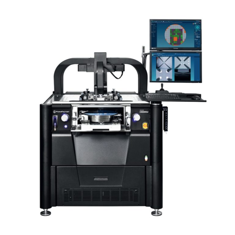
Equipment features: 1. Non-destructive precision testing Micrometer-level probe contact technology...