Chiplets packaging offers significant advantages over traditional multi-chip modules by enabling modular, cost-effective, and high-yield designs for advanced nodes. It allows decoupling process nodes, optimizing yields via smaller dies, and reusing validated IP blocks for faster innovation. DEEPETCH enhances chiplet performance with proprietary silicon interposers, ultra-fine RDLs, high-speed interconnects, and thermal-aware designs. Their solutions accelerate time-to-market through parallel development, prototyping with pre-validated chiplets, and streamlined supply chains. Supported by standardized interfaces (e.g., UCIe) and a collaborative ecosystem, DEEPETCH’s scalable platforms ensure long-term benefits for AI, 5G, and automotive applications, backed by proven reliability and high-yield production.
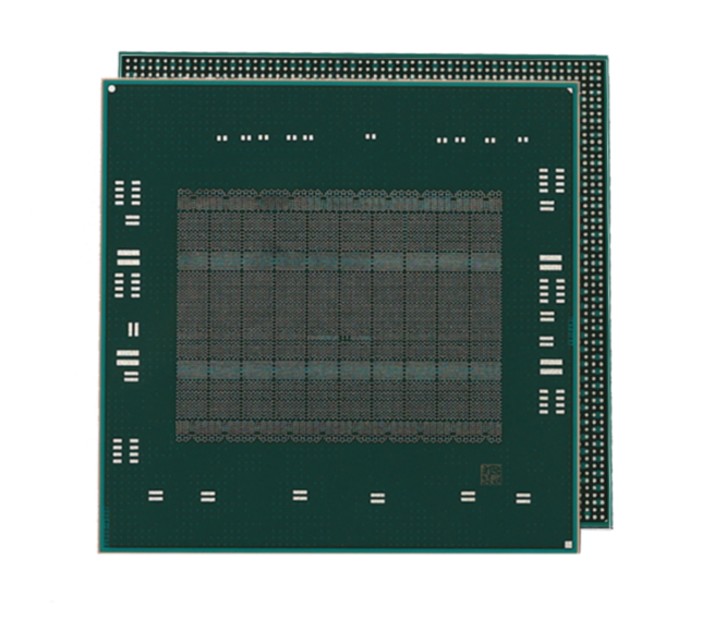
Building advanced chips is getting harder. Monolithic SoCs, which are single large chips, face problems with cost, defects, and complex designs. Chiplets Packaging offers a smart solution. It uses smaller, separate chips combined into one package. This method makes things more flexible and easier to build, especially for cutting-edge technology.
Chiplets Packaging lets you separate the chip’s design from the limits of one process node. For example, analog parts can stay on older, reliable nodes. Meanwhile, logic cores can use new tech like FinFET or GAA. This split lets each part use the best technology for its job. It keeps performance and power use in check. Plus, it speeds up new ideas and lowers risks when moving to newer nodes.
Breaking big chips into smaller chiplets boosts yield. Smaller chips have fewer flaws per wafer area. This means more working chips and lower costs for each function. At 5nm and smaller, defects are a big deal. With Chiplets Packaging, one bad chip doesn’t ruin the whole package. This makes production more efficient.
Chiplets Packaging has a big perk: reusing tested IP blocks. Instead of designing a whole new chip for every product, you can use proven chiplets in different setups. This saves time and money. It also keeps performance and reliability high. This reusable approach makes scaling easier.
To make Chiplets Packaging work well, you need advanced packaging tech. That’s where Deepetch Semicon Group Co., Ltd. (hereinafter referred to as “DEEPETCH”) shines. They lead in high-density connections and mixed-chip platforms for AI, HPC, 5G, and cars.
DEEPETCH has its own silicon interposer tech. It’s the core of their 2.5D packaging platforms. These interposers handle super tiny wiring and fast connections needed for modern chiplet systems.
DEEPETCH’s RDLs go down to sub-2µm line and space sizes. This means tight wiring between chiplets without signal loss or interference. It’s key for heavy data tasks like AI accelerators and network chips.
DEEPETCH’s micro-bump tech supports data speeds over 112Gbps per lane. It has low signal loss and little jitters. These connections are vital for fast tasks that can’t afford delays.
Through-silicon vias (TSVs) let chips stack vertically and deliver power well. DEEPETCH offers TSV setups you can tweak for heat or data needs. They ensure the package stays strong.
DEEPETCH plans for the future with mixed-chip integration. They combine different chips like logic, memory, RF, and analog on one platform.
You can package SRAM or DRAM with processors or analog parts on one base. This cuts delays and improves signal quality across different chip types.
DEEPETCH’s platforms scale well. They’re great for AI chips or HPC accelerators needing lots of parallel work and fast links between compute parts.
Heat is a big issue in dense chiplet packages. DEEPETCH uses heat-smart planning tools and special materials to manage hot spots. This keeps packages reliable for a long time.
Reliability matters for critical uses like cars or data centers. DEEPETCH ensures their packages are tough.
Every new platform gets strict testing in DEEPETCH’s labs. They check electrical performance to meet design goals before customers use them.
Packages go through tough tests like heat cycles, humidity, electrical stress, and shock tests. This ensures they last a long time.
DEEPETCH provides tools to check designs early. You can test heat, signal behavior, and package stress before building. This saves time and avoids costly fixes.
Getting products out fast is key in today’s chip world. Chiplets Packaging speeds things up by working on design and production at the same time.
Teams can work on different chiplets, like compute cores or memory controllers, at the same time. They don’t need to wait for the whole chip design to be done. This cuts delays a lot.
Using tested chiplets, called known-good-dies (KGDs), you can build prototypes quickly. You don’t need to make a whole new chip from scratch. This makes testing new ideas faster.
Chiplet designs make supply chains easier. You can get chips from different factories. This lets you mix and match parts while keeping control over the final package. It helps you respond to market needs or part shortages quickly.
A strong chiplet ecosystem drives new ideas. It’s growing fast thanks to standard rules and teamwork.
The Universal Chiplet Interconnect Express (UCIe) is an open standard. It ensures chips from different companies work together. This lowers risks and gives you more supplier choices. It’s like a plug-and-play system for chips.
Chip makers, tool providers, and assembly partners work together. This teamwork makes the process smoother, from design to mass production. It lowers risks during big projects.
DEEPETCH joins open groups to push chiplet tech forward. They help with design methods and heat simulation tools. This keeps you ahead in adding new features to your products.
Partnering with DEEPETCH sets you up for future-ready chip designs. Their solutions work for AI, 5G, cars, and more.
As AI and 5G tasks get tougher, modular designs are a must. DEEPETCH’s platforms support fast memory access and low-delay compute. This flexibility handles changing software needs.
You can add more compute chips or stack memory layers. DEEPETCH’s 2.xD platforms let you adjust setups without redesigning everything. This is great for updating hardware based on real-world data.
DEEPETCH has worked with top companies worldwide. They deliver consistent quality even with tiny chips. Their strict testing meets tough standards like AEC-Q100/200 for cars.
Q1: What differentiates chiplets from traditional multi-chip modules (MCM)?
A: MCMs combine separate chips with limited data links. Chiplets use fine connections for tight teamwork, like a single chip but with modular perks.
Q2: How does thermal management work in dense chiplet designs?
A: Heat-smart planning and special materials like TIMs or heat spreaders manage hot spots. Active cooling may be used for high-power chips in tight spaces.
Q3: Can I mix foundry sources when designing with chiplets?
A: Yes. You can use chips from different factories. They just need to follow standards like UCIe or DEEPETCH’s bridge formats.

The DE-CW-1310 DFB EPI wafer, a high-performance epitaxial structure designed for distributed feedback (DFB) lasers operating at 1310 nm....

Ceramic thin-filmvacuum sensor Optical gas massflowmeter Liquid mass flowmeter Force sensor MEMS...

Photoelectric sensing chip Light source chips Optical transmission and modulationchips Optical detection and receptionchips...

Using a“Detach Core”which has two-layers carrier foil structure on the surface as a core, and forming...

Tenting process is a kind of subtractive process, the process as follows: Laminating photosensitive film...

Modified Semi-Added Process abbreviated as mSAP, which can be used on the core or build-up layers, pattern...

Semi-Added Process abbreviated as SAP, using on the build-up-layer pattern forming as follow:First depositing...

The product generally adopts the pressing lamination process of semi-curing sheets , and line formation...

The products generally adopt the Build-up Film Lamination process, and the circuit formation uses the...

Equipment features: 1. Non-destructive precision testing Micrometer-level probe contact technology...