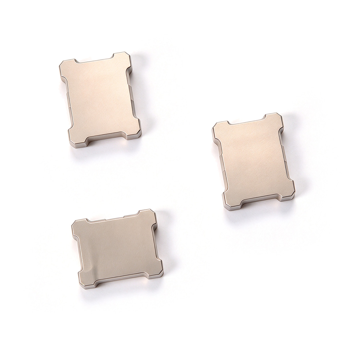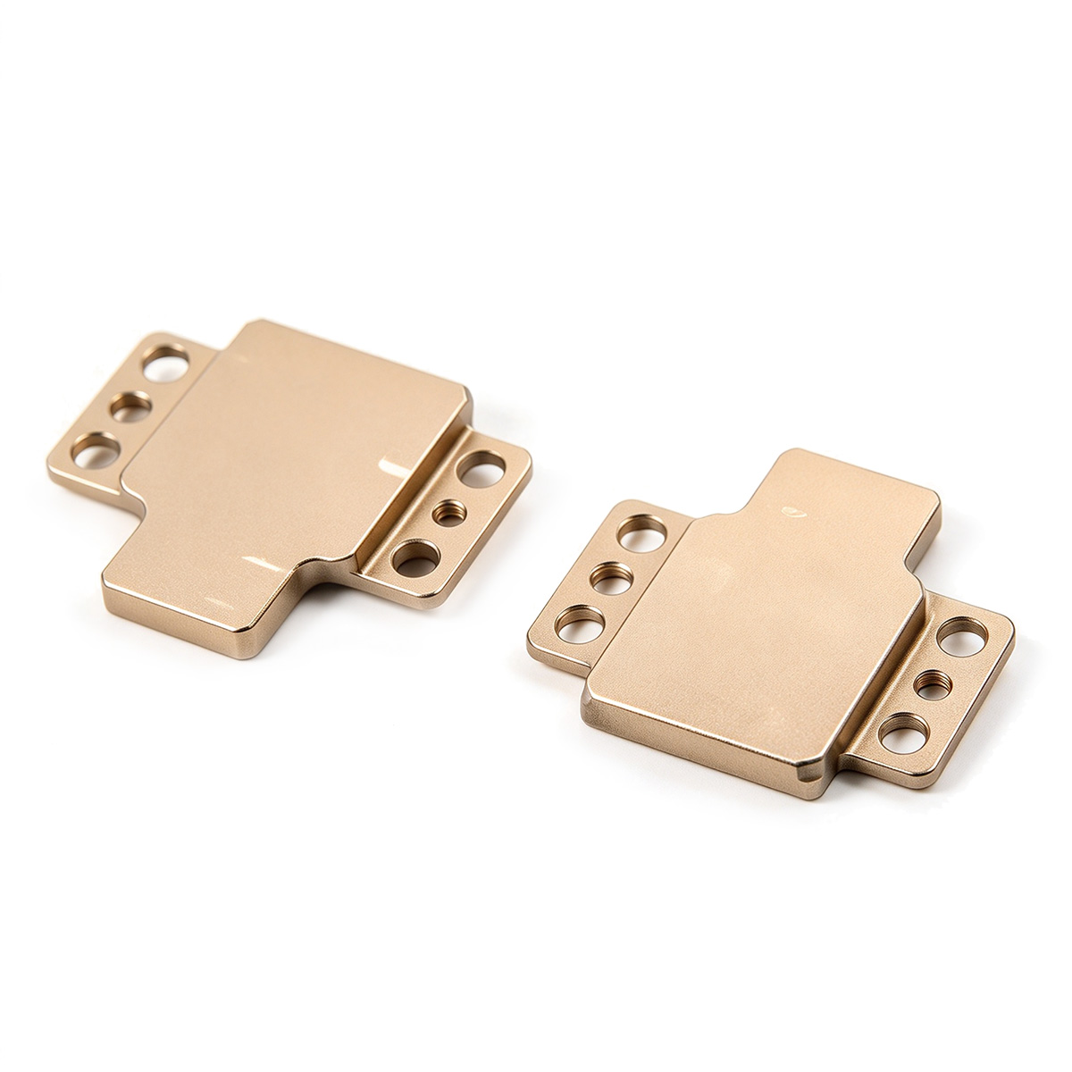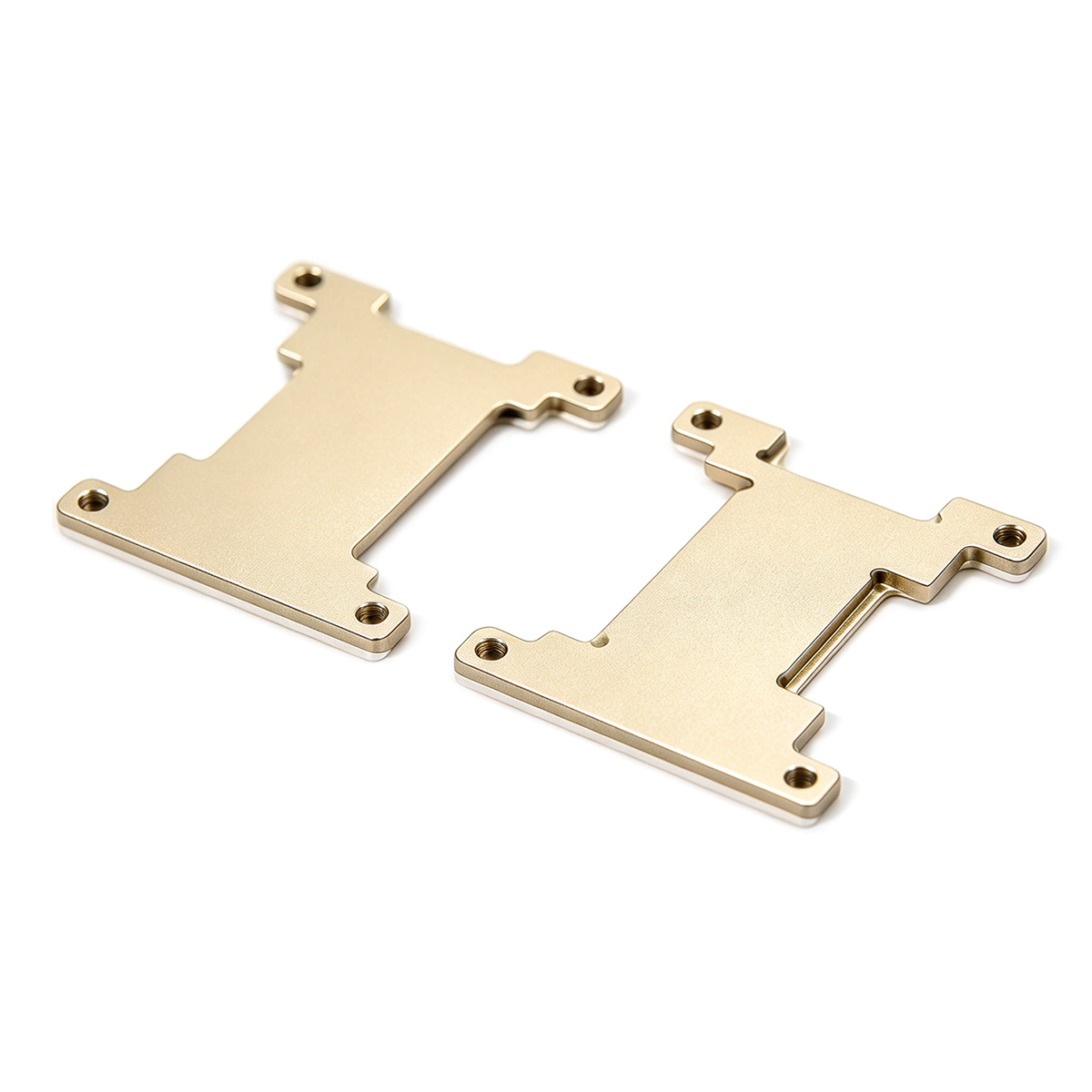
Molybdenum copper is a composite material of molybdenum and copper, Its performance is similar to that of tungsten copper, and it also has adjustable thermal expansion coefficient and thermal conductivity. However, the density of molybdenum copper is much smaller than that of tungsten copper, making it more suitable for aerospace and other fields.
| Product Name | Component | Average linear expansion coefficient [ppm/K] RT~400℃ | Thermal conductivity [W/(m·k)] | Mass Density [g/cm³] | Relative density [%T.D.] |
|---|---|---|---|---|---|
| Mo85 | Mo85Cu15 | 6.0~7.0 | ≥ 140 | 10.0 ± 0.2 | ≥ 99 |
| Mo80 | Mo80Cu20 | 6.5~7.5 | ≥ 150 | 9.9 ± 0.2 | ≥ 99 |
| Mo70 | Mo70Cu30 | 6.7~8.2 | ≥ 170 | 9.7 ± 0.2 | ≥ 99 |
| Mo65 | Mo65Cu35 | 7.8~9.3 | ≥ 180 | 9.65 ± 0.2 | ≥ 99 |
| Mo60 | Mo60Cu40 | 8.5~9.5 | ≥ 190 | 9.6 ± 0.2 | ≥ 99 |
| Mo55 | Mo55Cu45 | 10.5~11.5 | ≥ 200 | 9.55 ± 0.2 | ≥ 99 |
| Mo50 | Mo50Cu50 | 10.5~11.5 | ≥ 200 | 9.5 ± 0.2 | ≥ 99 |
Aerospace & Flight Electronics – Thermal management components where weight reduction is critical.
RF & Microwave – Heat spreaders and packages for high-power amplifiers.
Power Semiconductors – Substrates and heat sinks for IGBT, SiC, and GaN modules.
Optical Communication – Laser diode and photodetector packaging.
Molybdenum copper composite: adjustable CTE, high conductivity, lower density than tungsten copper. No...
Tungsten copper composite: low CTE, high conductivity. Ideal for RF, power, optical packaging.
Diamond-aluminum composite for advanced thermal management. Lightweight, high thermal conductivity, low...

Diamond-Copper Thermally Conductive Composite. High thermal conductivity, tunable CTE, robust.

The DE-CW-1310 DFB EPI wafer, a high-performance epitaxial structure designed for distributed feedback (DFB) lasers operating at 1310 nm....

Ceramic thin-filmvacuum sensor Optical gas massflowmeter Liquid mass flowmeter Force sensor MEMS...

Photoelectric sensing chip Light source chips Optical transmission and modulationchips Optical detection and receptionchips...

Using a“Detach Core”which has two-layers carrier foil structure on the surface as a core, and forming...

Tenting process is a kind of subtractive process, the process as follows: Laminating photosensitive film...

Modified Semi-Added Process abbreviated as mSAP, which can be used on the core or build-up layers, pattern...
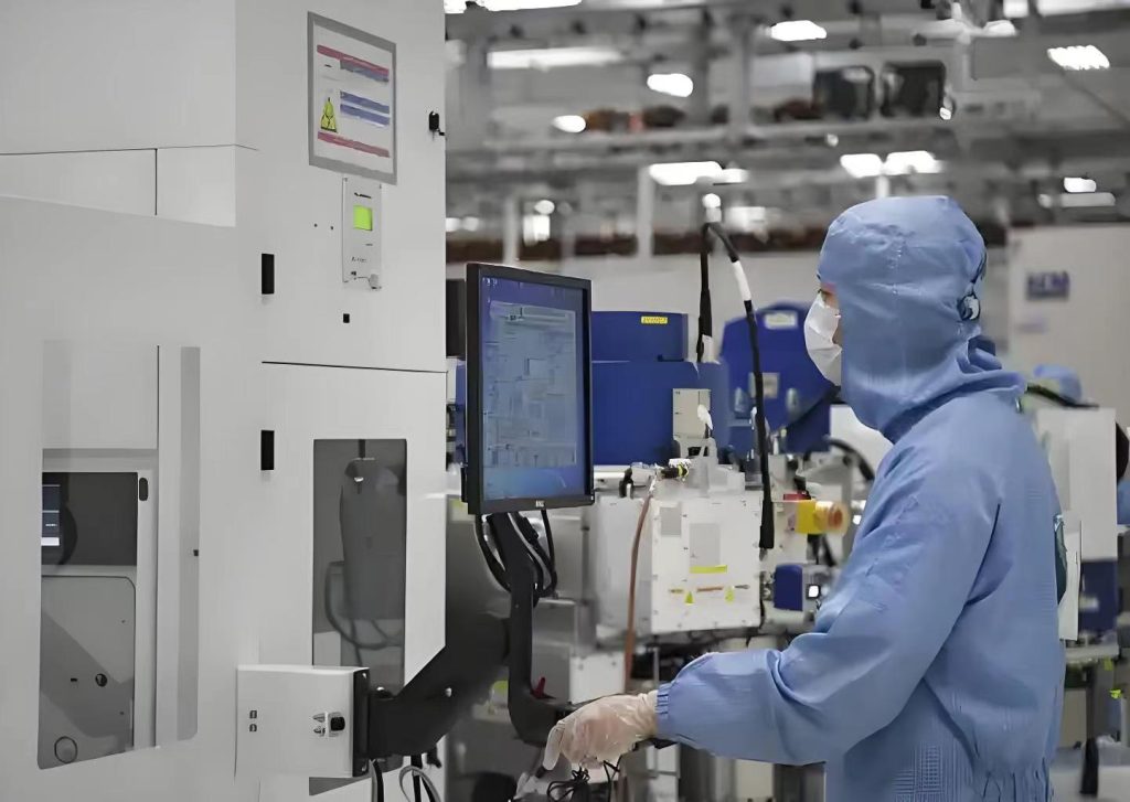
Supports advanced nodes such as [5-22nm FinFET/BCD/GAA] to meet the needs of high-performance computing (HPC), AI chips, etc.
MPW (Multi-Project Wafer) Service: Small batch trial production to reduce customers' initial costs. Customized process development: Cooperate with customers to conduct DTCO (Design-Process Co-Optimization), customize design rules and process parameters.
We support the joint solution of "wafer foundry + advanced packaging" (such as 3D IC, heterogeneous integration) to avoid the loss of multi-supplier collaboration. Unlike pure foundries, we verify the process stability through mass production of our own chips to reduce the risk of tape-out for you.
Electronic manufacturing services and printed circuit board assembly.
EMS provides a wide range of electronic manufacturing services, including everything from circuit board design to supply chain management to assembly, testing and after-sales support.
PCBA is a link in EMS that focuses on the assembly of printed circuit boards, covering component placement, soldering and related testing, connecting electronic components to manufactured printed circuit boards.
Title: Semiconductor manufacturing processes Objective: To have a certain foundation for the overall...