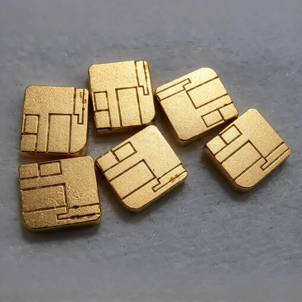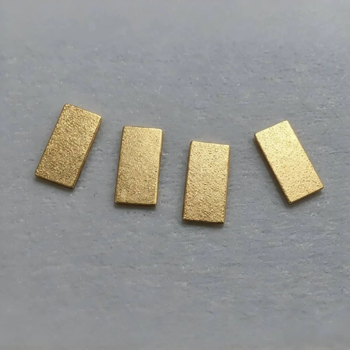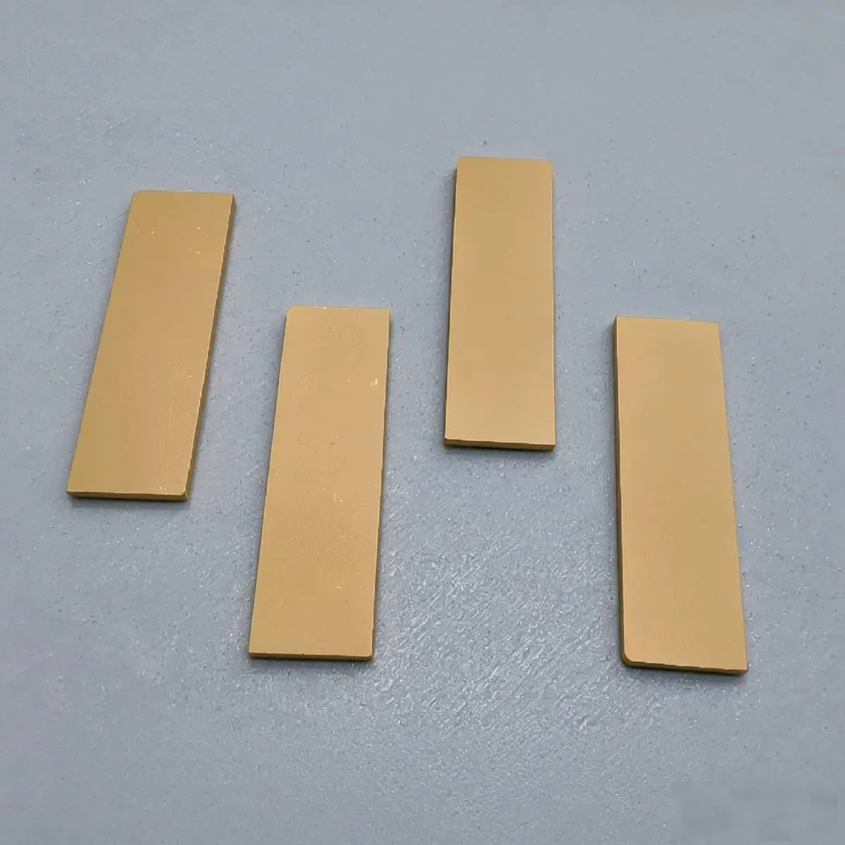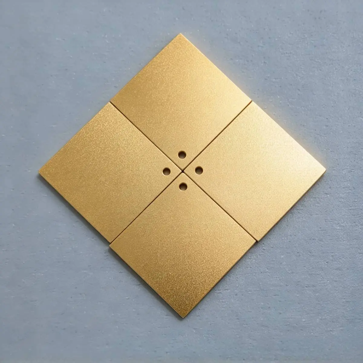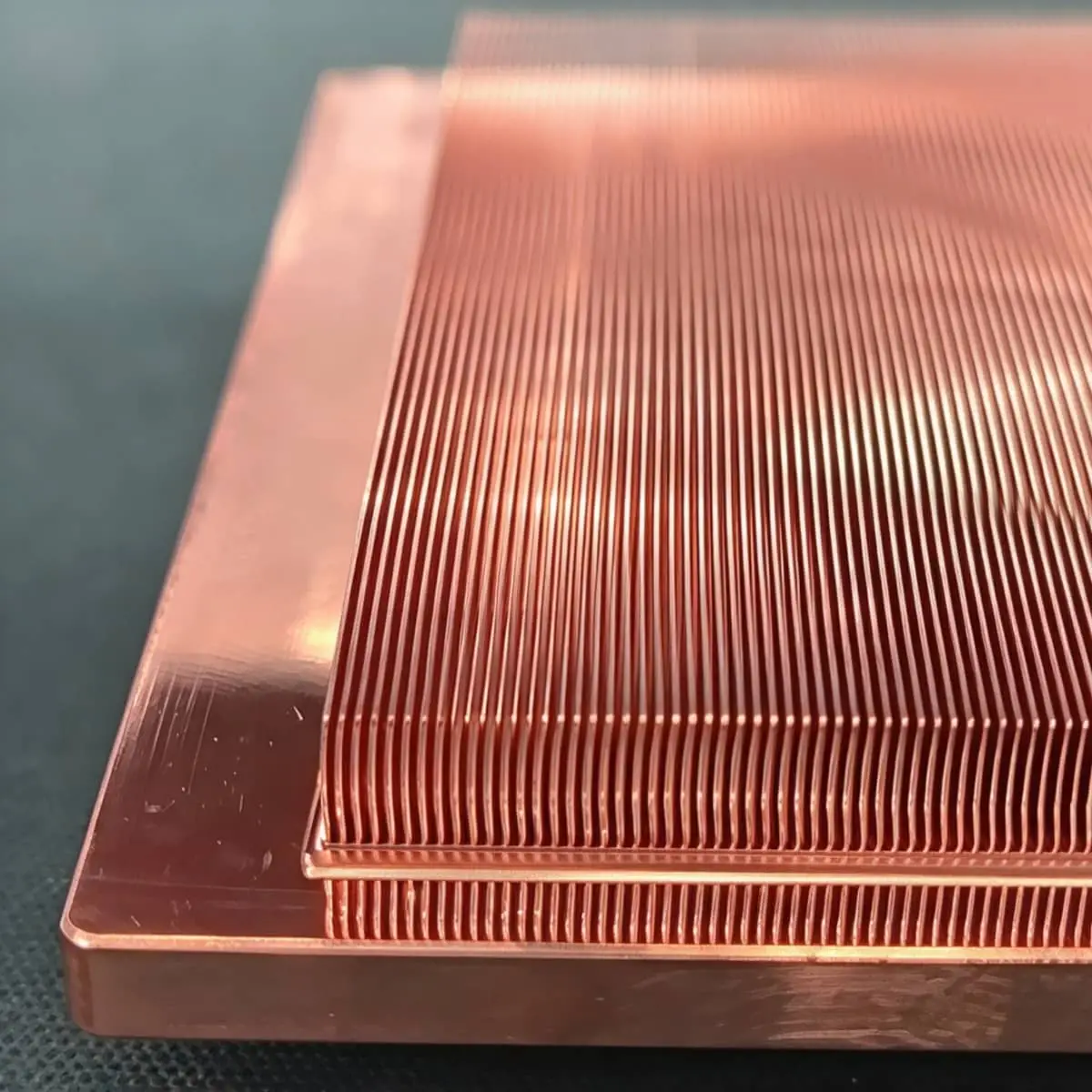


The SMARTNOBLE Diamond-Copper Thermally Conductive Composite is a high-performance material designed to solve the most demanding thermal challenges in modern electronic systems. By uniformly dispersing diamond particles within a copper matrix, this composite achieves a unique combination of ultra-high thermal conductivity, high mechanical strength, and a tunable coefficient of thermal expansion (CTE)—making it an ideal heat spreader and packaging material for high-power devices.
High Thermal Conductivity– Efficiently spreads and dissipates heat from high-power density devices such as IGBTs, GaN transistors, laser diodes, and high-brightness LEDs, reducing junction temperatures and extending service life.
High Strength – Provides excellent mechanical robustness, withstanding thermal cycling, vibration, and assembly stresses without cracking or deformation.
Tunable CTE – Can be tailored to match the CTE of common semiconductor materials (e.g., Si, GaAs, SiC, Al₂O₃, AlN), minimizing thermal stress and improving reliability in chip packaging and power modules.
Reliable Thermal Stability – Endures 1000 thermal shock cycles between -65°C and +150°C with less than 5% performance degradation, ensuring long-term reliability in harsh environments.
Customizable – Available in different thicknesses, thermal conductivities, and CTE values to meet specific design requirements.
Power Electronics – IGBT modules, SiC/GaN power devices, power converters, and inverters for electric vehicles and industrial drives.
Optoelectronics – High-power laser diodes, LED packaging, optical transceivers, and photodetectors.
RF & Microwave – GaN amplifiers, radar modules, and high-frequency power transistors.
Aerospace & Defense – Thermal management for avionics, satellite electronics, and high-reliability systems.
Semiconductor Packaging – Heat spreaders, lids, and substrates for high-performance processors and ASICs.
Research & Development – Advanced thermal management prototyping and material characterization.
Diamond-Copper Thermally Conductive Composite. High thermal conductivity, tunable CTE, robust.

The DE-CW-1310 DFB EPI wafer, a high-performance epitaxial structure designed for distributed feedback (DFB) lasers operating at 1310 nm....

Ceramic thin-filmvacuum sensor Optical gas massflowmeter Liquid mass flowmeter Force sensor MEMS...

Photoelectric sensing chip Light source chips Optical transmission and modulationchips Optical detection and receptionchips...

Using a“Detach Core”which has two-layers carrier foil structure on the surface as a core, and forming...

Tenting process is a kind of subtractive process, the process as follows: Laminating photosensitive film...

Modified Semi-Added Process abbreviated as mSAP, which can be used on the core or build-up layers, pattern...

Semi-Added Process abbreviated as SAP, using on the build-up-layer pattern forming as follow:First depositing...

The product generally adopts the pressing lamination process of semi-curing sheets , and line formation...

The products generally adopt the Build-up Film Lamination process, and the circuit formation uses the...
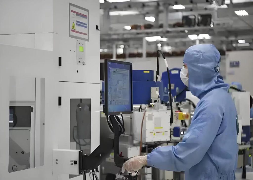
Supports advanced nodes such as [5-22nm FinFET/BCD/GAA] to meet the needs of high-performance computing (HPC), AI chips, etc.
MPW (Multi-Project Wafer) Service: Small batch trial production to reduce customers' initial costs. Customized process development: Cooperate with customers to conduct DTCO (Design-Process Co-Optimization), customize design rules and process parameters.
We support the joint solution of "wafer foundry + advanced packaging" (such as 3D IC, heterogeneous integration) to avoid the loss of multi-supplier collaboration. Unlike pure foundries, we verify the process stability through mass production of our own chips to reduce the risk of tape-out for you.
Electronic manufacturing services and printed circuit board assembly.
EMS provides a wide range of electronic manufacturing services, including everything from circuit board design to supply chain management to assembly, testing and after-sales support.
PCBA is a link in EMS that focuses on the assembly of printed circuit boards, covering component placement, soldering and related testing, connecting electronic components to manufactured printed circuit boards.
Title: Semiconductor manufacturing processes Objective: To have a certain foundation for the overall...