

For an IC Substrate purchase, start with the package role, size, bump pitch, routing density, layer build, material system, warpage limits, and assembly requirements. Then confirm that the supplier’s qualified process window, sample evidence, change control, quality documents, and commercial terms can support the specific revision. FCCSP, FCBGA, mSAP, and SAP are selection routes, not interchangeable labels.
DEEPETCH works around semiconductor substrate and optical communication material directions for buyers who need technical choices connected to manufacturable process paths. The buying decision should connect design inputs, process capability, sample feedback, and change control before a quotation is treated as comparable.
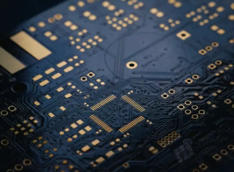
The substrate should be screened as a package interface, not selected from a product name alone. The first review should capture the following technical inputs.
Record whether the design is FCCSP, FCBGA, SiP, or another package route, together with package body size, bump pitch, die or interposer role, and assembly flow. These fields determine fan-out space, layer demand, handling sensitivity, and the downstream questions a supplier must answer.
Use the FCCSP Substrate when the package requires a compact form factor and controlled fine routing. Confirm the required line/space, bump pitch, stack-up, finished thickness, and assembly interface before treating a substrate option as feasible.
Routing pressure should be translated into minimum line/space, layer count, core or coreless structure, via technology, and copper build. DEEPETCH planning materials describe FCCSP fine-line capability at 8-12 um on SAP with 0.5 um base copper and 12 um on amSAP with 1.0 um base copper. One referenced FCBGA build is 14 layers, 45 x 45 mm unit size, 15/15 um minimum line/space, ABF-GL102 build-up material, and IVH with plugging and tenting in the core. These figures are screening references, not universal guarantees; confirm them against the revision-specific design and sample report, and ask which requirements are production-qualified versus sample-stage targets.
Request the material system, dielectric build, core or coreless structure, finished thickness, flatness or warpage criterion, measurement method, and assembly-side handling limit. A substrate that meets routing targets but fails during bonding, placement, or reflow is not a successful sourcing result.
Process route choice should follow design pressure and the supplier’s qualified window, not process-name fashion. The buyer should ask what design feature requires a route change and what risk remains after the change.
Traditional subtractive methods remain practical for many structures. They become less comfortable when trace width, spacing, sidewall control, or defect sensitivity approach the supplier’s process limit.
Ask where the current layout sits on the process map, which tolerances are controlled in production, and what inspection step detects an out-of-window feature. A lower-cost route is useful only when it remains stable through assembly and reliability testing.
mSAP is appropriate when the package needs tighter routing control than a conventional route can reliably provide but still fits the supplier’s qualified modified semi-additive window.
The mSAP Process is appropriate when the package needs tighter routing control than a conventional route can reliably provide but still fits the supplier’s qualified modified semi-additive window. Its commercial value comes from matching copper trace formation control to the actual design demand, not from using mSAP as a marketing label.
The SAP Process becomes relevant when finer feature formation, higher density, or structural requirements exceed the qualified mSAP window. Buyers should document the line/space, layer build, material system, inspection plan, and sample evidence that justify the route.
A useful comparison keeps engineering, purchasing, and assembly teams in the same conversation. Compare each option against the same technical, quality, delivery, and change-control fields.
| Buying question | What to ask | Why it matters |
| Package definition | FCCSP, FCBGA, SiP, package size, bump pitch | Keeps process choice connected to package role and assembly interface |
| Routing and stack-up | Minimum line/space, layer count, core/coreless build, via method | Shows whether the qualified mSAP or SAP window can support the design |
| Reliability and assembly | Material, finished thickness, warpage criterion, inspection plan | Connects substrate selection to downstream handling and yield |
| Supplier and commercial control | Sample timing, yield notes, MOQ, lead time, capacity, change rules | Prevents late technical or delivery surprises after quotation |
Use the same package, routing, material, reliability, delivery, and change-control questions for every candidate so that a process name does not hide a capability or schedule gap.
The FCBGA Substrate should be reviewed when a larger flip-chip BGA package, fan-out demand, thermal behavior, or assembly coordination is central. Compare package size, routing demand, material and thickness, downstream assembly risk, and sample evidence instead of forcing one substrate label into every project.

For additional reliability context, review why IC substrate manufacturers trust mSAP and SAP for long-term reliability. In the sourcing review, connect reliability to routing density, process capability, material behavior, inspection control, and the assembly condition rather than treating it as a process-name claim.
Sample-stage communication is where many sourcing risks become visible. The buyer should require traceable inputs, measurable results, and a clear decision when a sample does not meet the expected window.
The supplier should receive the package outline, stack-up, material requirements, layer and via information, line/space targets, bump map or assembly interface, drawing revision, and any thermal or warpage constraints. Ask which files are reviewed first and when manufacturability feedback will be returned.
A sample report should identify the design revision, process route, material lot or system, inspection items, measured results, open defects, and recommended revision. A simple good-or-bad statement is not enough for IC Substrate development.
If a sample shows a yield or reliability concern, the report should connect the symptom to routing density, material behavior, process step, or assembly condition. This turns a failed sample into a design decision instead of a vague supplier dispute.
Change control should define who receives a material, stack-up, routing, or process change and who must approve it before the next build. A change that seems minor to purchasing can affect assembly planning and reliability checks.
Before issuing an RFQ or purchase order, confirm package type and size, stack-up, minimum line/space, material, finished thickness, warpage criteria, inspection plan, sample schedule, MOQ, lead time, capacity, quality documents, and change-notification rules.
For a like-for-like supplier comparison, send the same revision-controlled input set to each candidate and record which assumptions remain open. A supplier that identifies missing information and ties its quotation to a sample plan is easier to manage than one that only confirms a broad capability statement.
Keep the approved input set, quotation assumptions, sample report, and change approvals together so that the purchase order remains traceable to the design revision being built.
IC Substrate buyers in 2026 should select a route only after package requirements, routing density, process capability, reliability risks, sample evidence, and commercial controls are connected. Use FCCSP, FCBGA, mSAP, and SAP as design-and-manufacturing choices tied to a revision-controlled data set. If a supplier cannot explain the process window, sample acceptance method, change rules, and delivery assumptions, the quotation is not ready for a like-for-like comparison.
If your team is reviewing IC Substrate options, process-route questions, or advanced packaging project requirements, send the design and sourcing details through contact page.
Advanced packaging places more pressure on package size, routing density, layer build, warpage, reliability control, and supplier communication. Buyers therefore need a qualified process window and traceable sample evidence, not only a product label.
Discuss mSAP or SAP when the required line/space, density, layer build, or structural control exceeds what a simpler qualified route can support. The decision should be backed by the design revision and sample evidence.
Compare package type and size, bump pitch, routing and layer requirements, material and thickness, warpage and assembly risk, process capability, sample results, quality documents, delivery terms, and change-control discipline.

The DEEPETCH DP-QPA2611 is a high-performance X-Band (8–12 GHz) Gallium Nitride (GaN) Power Amplifier...

The DEEPETCH DP-ROS-40121 is a premium, solvent-free epoxy die attach adhesive engineered for the most...
The Diamond Heat Spreader is a highly efficient thermal management material engineered for the most demanding...
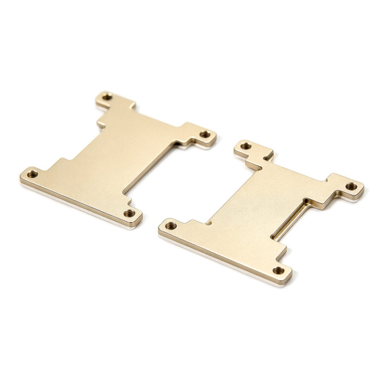
Molybdenum copper composite: adjustable CTE, high conductivity, lower density than tungsten copper. No...
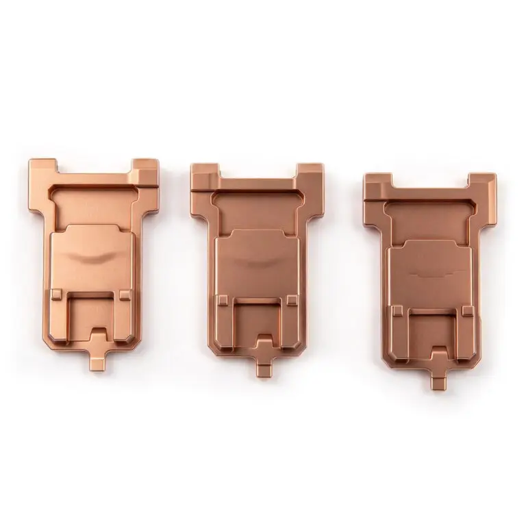
Tungsten copper composite: low CTE, high conductivity. Ideal for RF, power, optical packaging.
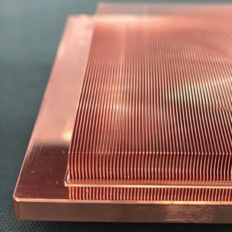
Diamond-Copper Thermally Conductive Composite. High thermal conductivity, tunable CTE, robust.
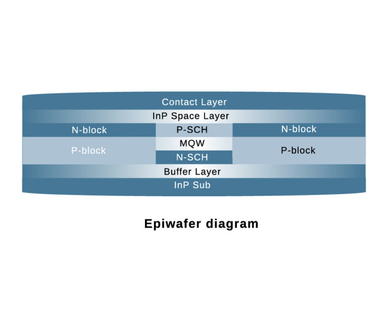
The DE-CW-1310 DFB EPI wafer, a high-performance epitaxial structure designed for distributed feedback (DFB) lasers operating at 1310 nm....
Ceramic thin-filmvacuum sensor Optical gas massflowmeter Liquid mass flowmeter Force sensor MEMS...
Photoelectric sensing chip Light source chips Optical transmission and modulationchips Optical detection and receptionchips...
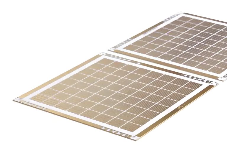
Using a“Detach Core”which has two-layers carrier foil structure on the surface as a core, and forming...