

DP-QPA2611 X-Band GaN PA MMIC

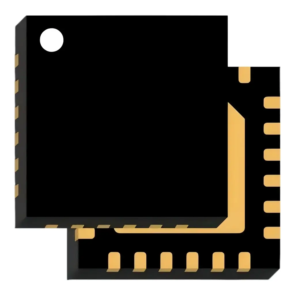
The DEEPETCH DP-QPA2611 is a high-performance X-Band (8–12 GHz) Gallium Nitride (GaN) Power Amplifier MMIC, manufactured using an advanced 0.15μm GaN-on-SiC process. Delivering a saturated output power of 5W (>37 dBm) with exceptional power-added efficiency (PAE >42%), it is the ideal building block for next-generation Active Electronically Scanned Arrays (AESA). Housed in a compact 5×5 mm QFN package, it features integrated DC blocking capacitors at the I/O ports and 50Ω internal matching, drastically simplifying external circuitry and reducing the overall size of phased array T/R modules.

(Note: The DP-QPA261x family also includes DP-QPA2610 (3W) and DP-QPA2612 (12W). Datasheet specifications are based on pulsed conditions. For CW operation, proper derating and enhanced thermal management are required.)

DP-QPA2611 X-Band GaN PA MMIC

Product album display

Key Features

•  QGaN15 GaN-on-SiC process , wideband X-band, suitable for phased array T/R modules.

•  Integrated DC blocking capacitors, simplifying external matching circuits and reducing phased array face size.

•  High PAE, reducing array power consumption and thermal stress.

•  Evaluation board available: DP-QPA2611EVB.


X-Band GaN PA MMIC Core Specifications

Item Specification
Frequency Band 8 ~ 12 GHz (X-Band)
Saturated Output Power (Psat) 5 W (>37 dBm), P1dB ≈ 38 dBm
Small-Signal Gain 26 dB (Typical), up to 35 dB under certain conditions
Drain Voltage (Vd) 24 V
Quiescent Drain Current (Idq) 105 mA
PAE > 42%
Package 5×5 mm QFN, 24-pin, I/O ports integrated DC blocking capacitors, 50Ω matched
Gate Voltage Range (Vg) −4V ~ 0V (Negative gate bias)
Storage Temperature −55 ~ +150℃; MSL3
chip

Application Areas

•  X-Band Active Electronically Scanned Array (AESA) radar

•  Electronic warfare jamming sources

•  X-Band satellite communications, point-to-point microwave communications

IDM Customization Service

From advanced processes to specialty processes, we use our IDM vertical integration experience to help customers overcome design-process collaboration challenges.

01

Supports advanced nodes such as [5-22nm FinFET/BCD/GAA] to meet the needs of high-performance computing (HPC), AI chips, etc.

02

MPW (Multi-Project Wafer) Service: Small batch trial production to reduce customers' initial costs. Customized process development: Cooperate with customers to conduct DTCO (Design-Process Co-Optimization), customize design rules and process parameters.

03

We support the joint solution of "wafer foundry + advanced packaging" (such as 3D IC, heterogeneous integration) to avoid the loss of multi-supplier collaboration. Unlike pure foundries, we verify the process stability through mass production of our own chips to reduce the risk of tape-out for you.

Provide customers with complete integrated manufacturing services from concept to finished product

01

Electronic manufacturing services and printed circuit board assembly.

02

EMS provides a wide range of electronic manufacturing services, including everything from circuit board design to supply chain management to assembly, testing and after-sales support.

03

PCBA is a link in EMS that focuses on the assembly of printed circuit boards, covering component placement, soldering and related testing, connecting electronic components to manufactured printed circuit boards.

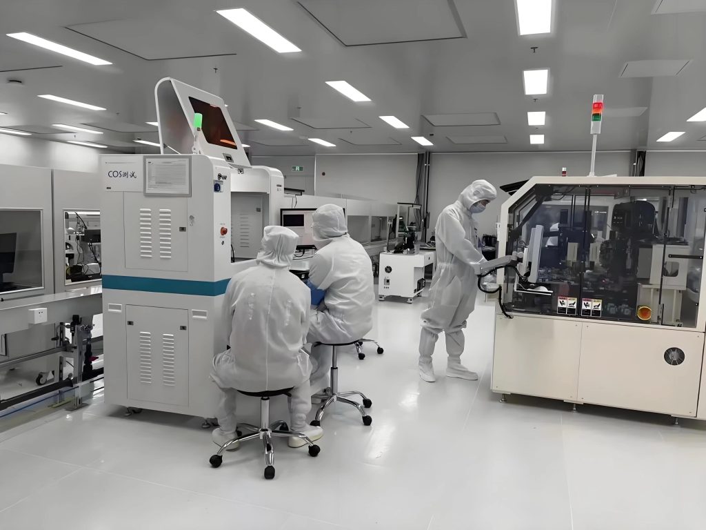
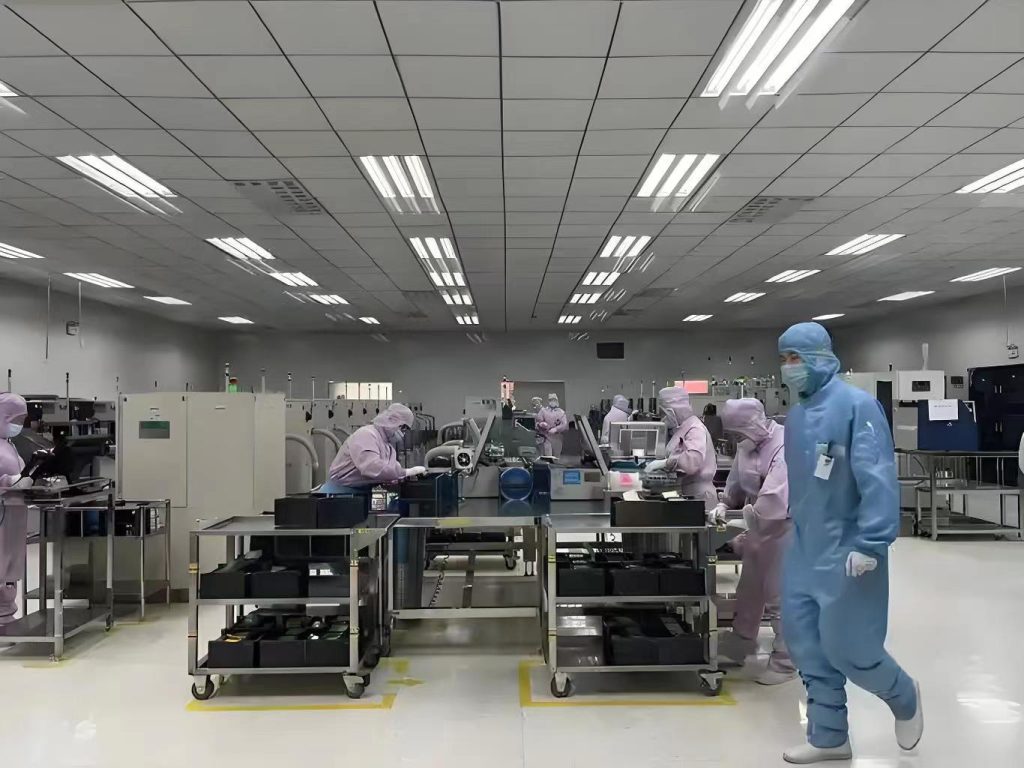
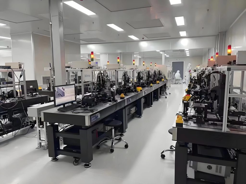
Semiconductor production shop environment

News Center