
The die attach material is the joint that sets three things at once: how much of the die temperature you can run, how the joint survives thermal cycling, and whether you can ever rework the package. For high-temperature and high-power semiconductor packages, choosing it wrong shows up later as a lower junction-temperature margin, a cracked interface, or a die you cannot recover.
This article walks the selection in the order the decisions actually happen: temperature and power first, CTE and the thermal path second, reliability and rework third, then the process. The examples assume a power or high-current die on a metal or ceramic submount, but the same decision tree applies to RF, optics and sensing packages with different numbers.
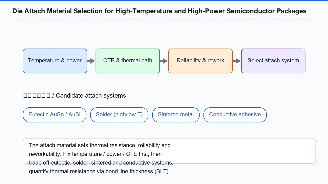
Every attach system has a ceiling. Conductive adhesives are the room-temperature workhorse, with useful service ranges that stop well short of the high-temperature end of a power package. Solder systems cover the middle: low-melting alloys for reworkable, moderate-temperature joints, and higher-melting alloys (SnAgCu family and leaded high-T solders) when the operating range is higher. Eutectic bonds (AuSn, AuSi) sit at the top of the temperature ladder and are the standard for high-current power and RF dies. Sintered silver and other sintered metals are the newer high-temperature option where you also want the lowest possible bond-line thermal resistance.
The number to write down is not ‘high temperature’ but the operating junction and case range, the power at that range, and the lifetime. A 150 C case at 2 W is a different attach problem from a 60 C case at 20 W, even though both feel ‘high power’ in a meeting. The die attach material’s melting point or softening point must sit above the operating range with the margin the reliability plan requires, and that margin is part of the specification, not an assumption.
The attach layer sits between two materials that expand at different rates. Every thermal cycle puts that mismatch into shear and peel stress at the interface. A high-CTE die on a low-CTE ceramic submount cycles harder than the same die on a copper or Kovar submount, and the interface is where the stress concentrates. The Aluminum Nitride (AlN) submount you chose for its thermal conductivity also has a low CTE, and that is why it is a good pairing candidate for a high-power die, not a contradiction of it.
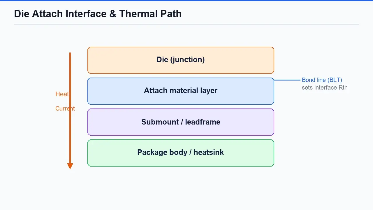
Thermal resistance is the second number. The bond line is part of the heat path from junction to case, and its resistance scales with bond-line thickness (BLT). A thinner, denser joint lowers Rth, which is one of the arguments for sintered or eutectic at the high-power end; a thicker adhesive layer does the opposite. The die attach material you choose therefore sets both the temperature ceiling and the Rth of the path, which is why the CTE and the thermal decision should be made on the same sheet, not in two emails.
| Attach system | Typical service range | Thermal resistance | Rework | Typical role |
| Conductive adhesive | Low / moderate | Higher (thicker line) | No | Low-power, signal-path packages |
| Solder (low-T) | Moderate | Medium | Yes | Reworkable mid-power designs |
| Solder (high-T, SnAgCu / leaded) | High | Medium | Limited | High-temperature power |
| Eutectic AuSn / AuSi | Very high | Low | Limited | High-current power, RF |
| Sintered metal | Very high | Lowest | Limited | Max thermal + max temperature |
Ranges in the table are indicative, for structuring the decision; the exact service range comes from the material’s datasheet and your qualification plan. Do not carry a ‘typical’ range into a reliability commitment.
The die material sets part of the problem. A GaAs, InP or SiC die has a different CTE from the submount than a Si die does, and the same is true of the metallization that the attach actually wets. For a high-power design on ceramic, the pairing question is ceramic-versus-die CTE plus the metallization chemistry, which is why a ceramic CBGA style housing and an AlN or alumina submount get specified together rather than independently.
The environment sets the rest: temperature cycling range and rate, humidity or hermeticity, vibration, and the lifetime in years. A package that runs hot in a ground vehicle and a package that runs the same hot in an aerospace environment are the same attach temperature and different attach problems. If the die itself is a device with processed layers, the Deep RIE system page shows where the front-end process ends and the attach decision begins.
Reliability is where ‘good thermal numbers’ stop being enough. The attach system has to pass the package’s qualification: thermal cycling, temperature-humidity bias, highly accelerated stress test, and lifetime at the operating point. A joint that is electrically clean at bond and fails at cycle 2000 is not a pass, and the failure mode at the interface (crack, delamination, Kirkendall voids) tells you which of the earlier decisions was wrong.
Rework changes the economics. An adhesive bond is the cheap part of a bad assembly; a eutectic or solder joint on a high-power die is not. If yield risk is high at the start of a design, a reworkable attach on the first articles is a legitimate trade, with the permanent system chosen for production. On the equipment side, the bond itself is a temperature, force and atmosphere recipe, and the DEEPETCH wire & die bonder line and broader packaging equipment line cover the process station where that recipe lives.
The checklist is short, and every line is one of the decisions above: die and submount materials with CTE values, power at the operating point and the junction-temperature limit, temperature range and cycling profile, lifetime and environment, rework requirement, and target BLT with the thermal-resistance budget. Send it with the submount drawing, mark the open items, and the attach recommendation you get back can be checked against your numbers instead of against a generic ‘high-power’ label.
DEEPETCH can carry that package as a set: the submount material line, the ceramic housing, and the process equipment that attaches the die. Send DEEPETCH the checklist with the submount drawing and the open items marked, and the attach system you get back is one you can hold to in qualification.
A No. A higher melting point buys temperature margin, but it costs reworkability and can shift the process window. Match the melting point to the operating range plus the reliability margin, not to the maximum the material can take.
Sometimes, when the temperature ranges overlap. Usually not: a sensor package may tolerate an adhesive that a power die cannot, and the CTE pairing is different for each. Specify per die, and share the submount if the environment allows it.
Give the target BLT and the thermal-resistance budget, and let the bonding recipe hit both. A BLT number alone means little without the Rth target, because the process trades fill and thickness against voiding.
Die and submount materials, power and junction-temperature limit, temperature range and cycling profile, lifetime and environment, rework requirement, and the BLT / Rth budget. Send it with the submount drawing and the open items marked.

Diamond-Copper Thermally Conductive Composite. High thermal conductivity, tunable CTE, robust.

The DE-CW-1310 DFB EPI wafer, a high-performance epitaxial structure designed for distributed feedback (DFB) lasers operating at 1310 nm....

Ceramic thin-filmvacuum sensor Optical gas massflowmeter Liquid mass flowmeter Force sensor MEMS...

Photoelectric sensing chip Light source chips Optical transmission and modulationchips Optical detection and receptionchips...

Using a“Detach Core”which has two-layers carrier foil structure on the surface as a core, and forming...

Tenting process is a kind of subtractive process, the process as follows: Laminating photosensitive film...

Modified Semi-Added Process abbreviated as mSAP, which can be used on the core or build-up layers, pattern...

Semi-Added Process abbreviated as SAP, using on the build-up-layer pattern forming as follow:First depositing...

The product generally adopts the pressing lamination process of semi-curing sheets , and line formation...

The products generally adopt the Build-up Film Lamination process, and the circuit formation uses the...