
A wafer can pass electrical test and still lose usable dies during separation. Edge chips, cracks, contamination and pickup damage all matter, but they do not necessarily come from the same step. Before changing the saw recipe, establish where the damage first appears.
Wafer dicing separates a processed wafer into individual dies. Blade cutting, laser processes and plasma dicing remove or separate material in different ways. The right choice depends on the wafer material, thickness, street layout, film stack and acceptable edge condition. For blade dicing, controlling chipping requires a matched blade, cutting recipe and support system, followed by inspection of both wafer faces and the downstream pickup result.

The drawing identifies inspection locations and possible defect types. The subsurface crack is shown conceptually to explain the risk; an ordinary top-view optical image cannot rule out hidden damage. No acceptance dimensions are implied.
The dicing street is the area allocated between neighboring dies. The kerf is the material removed by the cut. These widths are related but not identical. A blade that fits within the nominal street still needs allowance for alignment error, kerf variation and the permitted damaged region.
Read the layout with the device engineer. Streets can contain metal, test structures or other films that behave differently from the underlying silicon. Identify the active-area keep-out boundary and any seal-ring restrictions. Do not derive an acceptable chip size simply by subtracting the blade width from the street width.
Thickness is equally important. The incoming wafer, the wafer after grinding and the finished die may have different handling requirements. If thinning precedes singulation, review the backgrind finish and the support condition at the saw. DEEPETCH’s wafer thinning equipment can be discussed as part of the upstream process scope, but the dicing trial must use the specified final thickness and surface condition.
The acceptance drawing should distinguish frontside chipping, backside chipping, cracks and film damage. Record the measurement reference, inspection method and sampling coverage. “No excessive chipping” is not a reproducible acceptance criterion.
Blade dicing uses a rotating abrasive blade to cut along the streets. It is a practical starting point when the material stack, cooling and mechanical loading are compatible. Qualification still needs representative wafers, not just a bare material coupon.
Laser ablation removes material along a path and can be considered when a mechanical blade is unsuitable. Review debris, local thermal effects and the response of each film in the street. Do not group all laser methods under one set of assumptions.
In internal laser modification, often called stealth dicing, the beam creates a modified region inside a suitable material and a later separation step opens the dies. This requires appropriate optical access and material response. It is different from ablating a groove at the surface, and suitability must be demonstrated for the actual wafer stack.
Plasma dicing etches exposed streets, commonly using a patterned mask. It can avoid direct blade contact with the die edge, but mask preparation, street materials, etch compatibility and tape handling become part of the process. A generic etcher specification does not establish a complete qualified singulation flow.
| Candidate process | Main separation mechanism | Key qualification questions |
| Blade dicing | Mechanical abrasive cutting | Blade match, chipping, coolant, tape support |
| Laser ablation | Local material removal | Film response, debris, thermal damage |
| Internal laser modification | Internal modification and subsequent separation | Optical access, crack path, separation and pickup |
| Plasma dicing | Etching through exposed streets | Mask and film compatibility, sidewall quality, handling |
These are screening questions, not a ranking. A process that performs well on one wafer type may need a different flow for another. Hybrid approaches also exist, but every added operation needs its own alignment and acceptance checks.
Choosing the finest abrasive is not a complete chipping strategy. Finer grit can reduce individual abrasive impacts, while films or street structures may load the blade and change its cutting behavior. Blade bond, thickness, exposure, wear condition and dressing procedure all affect the trial.
Feed speed and spindle speed must be evaluated together with that blade. Slowing the feed is not guaranteed to improve a thin-wafer process. The blade still needs a suitable operating load and cutting condition. Start within the equipment and consumable suppliers’ approved ranges, then compare controlled trials. Do not copy settings from a different material or thickness because the first cut looks clean.
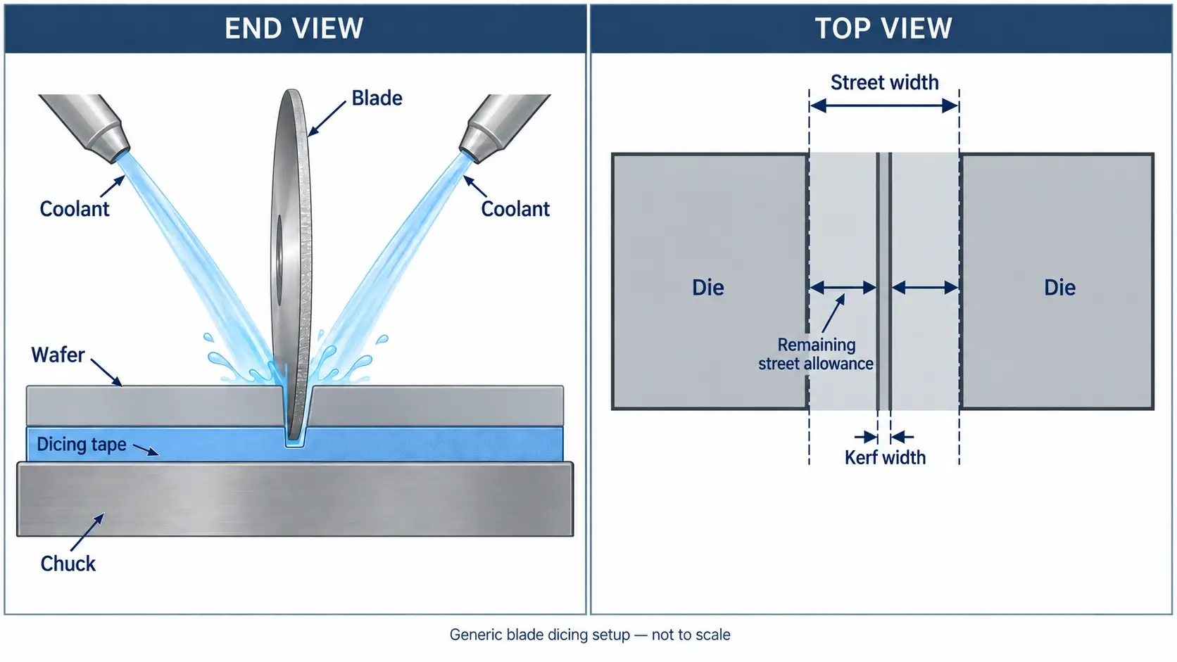
The setup is a generic schematic, not an equipment specification. The blade enters the qualified tape depth without cutting through the support tape. Actual depth settings and allowances must come from the mounting stack and validated process.
For DEEPETCH’s automatic dicing saw, ask which configuration is proposed for the wafer, blade and frame combination. Confirm the alignment system, height measurement, coolant arrangement and inspection functions included in the quotation. An equipment feature list should lead to a test plan, not substitute for one.
Poor tape contact can leave a locally unsupported area beneath the wafer. Check for trapped particles, bubbles, uneven lamination or handling damage before attributing every edge defect to cutting speed. Inspect the chuck and frame setup as well as the wafer itself.
Blade depth deserves a separate check. A full-cut process normally needs to separate the wafer while leaving the supporting tape usable. The correct allowance depends on actual wafer thickness, tape construction, mounting flatness and height-control accuracy. Too little depth can leave incomplete separation. Excess depth can damage the support and complicate handling.
Coolant has to reach the cutting region and carry debris away. Check nozzle position and flow under the intended setup, along with water quality and device-specific contamination controls. A nozzle can appear correctly placed while its delivery is obstructed by the blade configuration.
Finally, compare the first cuts with later cuts. A recipe may look acceptable on a fresh blade and deteriorate as material accumulates or the blade wears. Record blade condition, cut length and dressing events so that a drift in edge quality can be investigated rather than averaged away.
A useful trial records incoming condition, post-cut condition and post-pickup condition separately. Preserve wafer coordinates so that a damaged die can be traced back to its street and cutting sequence.
Inspect front and back edges using methods suited to the defect size and material. DEEPETCH’s AOI test equipment is a starting point for discussing automated visible-defect inspection. Confirm that the proposed optics and handling can see the relevant edges and surfaces. A clean top-side image does not establish that the backside or subsurface is undamaged.
Where hidden cracking or reduced mechanical strength is a concern, agree on appropriate additional analysis and strength or reliability tests. Electrical checks answer another part of the problem. Probe-station equipment may support the agreed measurements with suitable fixtures, but electrical continuity alone cannot certify mechanical edge integrity.
Keep inspection labels specific. Record a chip, crack, scratch, particle or delaminated film as the observed defect, with its location and measurement. The proposed root cause belongs in a separate field until a trial supports it.
Use wafers that represent the production stack, including street films and backside processing. Document the baseline recipe before changing it. Where several settings interact, plan the trial so those interactions can be evaluated instead of changing everything at once.
Include more than the best-looking region of one wafer. Examine different positions and cutting directions, plus the beginning and end of the planned blade-use interval. Set the number of wafers and dies with the process owner according to the risk and available material. There is no universal sample count that qualifies every wafer type.
Measure accepted dies after the relevant downstream steps. A faster cut is not a throughput improvement if it creates more inspection, cleaning or pickup loss. Likewise, a low visible chip count is insufficient if the die-strength result or device performance fails the specification.
Keep the raw defect images and coordinates, not just a pass percentage. They make it possible to distinguish a localized support problem from a gradual blade-condition change during the next trial.
Send a short, complete process package rather than asking only for a wafer diameter and machine price:
Mark unknown values explicitly. If the tape is still being selected, that decision belongs in the qualification scope. If a street contains a test structure, show it in the drawing rather than assuming the equipment supplier will infer it.
No. The limit depends on the device layout, protected structures, die thickness and subsequent loading. It must also specify how and where the defect is measured. A number without its measurement method and reference boundary cannot serve as a complete acceptance rule.
No. Thinness is only one input. Films, optical access, material response, surface requirements and pickup behavior can change the choice. Compare qualified results for the whole process, not a general claim that one cutting method produces a cleaner edge.
For a wafer dicing project, send DEEPETCH the wafer stack and acceptance drawing. Ask for a proposed configuration, representative cutting trial and inspection plan. Those three deliverables provide a practical basis for deciding whether the process is ready for the next stage.

The DE-CW-1310 DFB EPI wafer, a high-performance epitaxial structure designed for distributed feedback (DFB) lasers operating at 1310 nm....

Ceramic thin-filmvacuum sensor Optical gas massflowmeter Liquid mass flowmeter Force sensor MEMS...

Photoelectric sensing chip Light source chips Optical transmission and modulationchips Optical detection and receptionchips...

Using a“Detach Core”which has two-layers carrier foil structure on the surface as a core, and forming...

Tenting process is a kind of subtractive process, the process as follows: Laminating photosensitive film...

Modified Semi-Added Process abbreviated as mSAP, which can be used on the core or build-up layers, pattern...

Semi-Added Process abbreviated as SAP, using on the build-up-layer pattern forming as follow:First depositing...

The product generally adopts the pressing lamination process of semi-curing sheets , and line formation...

The products generally adopt the Build-up Film Lamination process, and the circuit formation uses the...
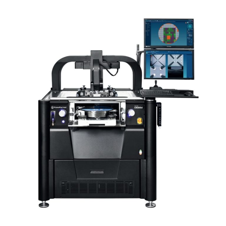
Equipment features: 1. Non-destructive precision testing Micrometer-level probe contact technology...