
A smaller die does not always produce an easier package. If the chip still needs the same number of connections, shrinking its area leaves less room for solder balls and board routing. That is often the point at which a packaging discussion turns from fan-in to fan-out.
Wafer level packaging brings interconnect and protective structures into wafer-scale processing. In a typical fan-in WLCSP, the external connections remain within the die footprint. Fan-out adds usable connection area beyond the die, commonly by embedding separated dies in mold compound and building redistribution layers across the reconstructed surface. Choose between them by checking the complete route from die pads to the PCB, then qualifying assembly and reliability. Neither name alone establishes cost or production readiness.

The drawing compares connection areas, not a production stackup. Its routing is deliberately simplified. Actual pad locations, dielectric layers and edge clearances come from the approved package design.
The redistribution layer, or RDL, moves electrical connections from the die’s original pads to the package connection pattern. It combines patterned conductors with insulating layers. That makes the external ball arrangement less dependent on the original die-pad layout, but it does not create unlimited routing space.
In fan-in wafer-level chip-scale packaging, the available area is constrained by the die. Fan-out creates additional area around it. This can provide more room for connections or accommodate a board-side pitch that would not fit on the die itself. A fan-out package can also contain multiple dies, although a single-die fan-out design is entirely possible.
The manufacturing sequence matters. A mold-first fan-out flow places dies on a temporary carrier and forms a reconstructed molded body before building the RDL. An RDL-first flow forms the routing before die attachment and subsequent encapsulation. The process supplier should identify the actual sequence being quoted, because the alignment, inspection and yield questions change with it.
| Decision point | Fan-in WLCSP | Fan-out WLP |
| Connection area | Usually limited to the die footprint | Extends beyond the die footprint |
| Initial design check | Can the ball map fit and escape on the PCB? | How much extra routing area is needed? |
| Manufacturing review | Wafer processing, bumping and singulation | Reconstruction, alignment, RDL and singulation |
| Assembly review | Board layout and solder-joint reliability | Board layout, package warpage and solder-joint reliability |
| Quotation basis | Exact die and ball-map requirements | Exact die set, package outline and process flow |
The table describes common architectures, not a universal specification. Package vendors use different names and variants. Request a cross-section and process flow before comparing quotations.
Start with the die outline and the complete list of required connections. Include power and ground balls, reserved pins and test-related requirements, not just signal I/Os. Then place the proposed ball pattern on the actual PCB stackup.
Can the board supplier escape the inner rows using the permitted trace widths and vias? Is there room for the required power return paths? Will assembly need a finer stencil or inspection process than the factory currently uses? A package that fits geometrically can still create an expensive board problem.
Consider a design revision that reduces die area while leaving the interface unchanged. Fan-in may force a finer ball pitch, a different ball map or a change to the PCB. Fan-out gives the package designer another option: retain additional connection area outside the smaller die. This is a design scenario, not proof that fan-out is cheaper. Compare the revised package and PCB together.
There is also a substrate-based alternative. DEEPETCH supplies FCCSP packaging substrates for flip-chip chip-scale packages. FCCSP uses a package substrate and should not be treated as another name for fan-in WLCSP. When both architectures are viable, ask for two clearly separated proposals with the same electrical, mechanical and reliability requirements.
An attractive routing drawing is only the starting point. Ask how the process holds the die position, maintains a usable surface for lithography and verifies the finished connections.
For a mold-first design, die movement during molding and the resulting alignment to the RDL deserve specific attention. For an RDL-first design, ask how routing integrity is checked before valuable dies are attached. In either case, inspection should have defined acceptance limits and a record of which units passed each stage.
Temporary support materials belong in this review. A carrier used during thin-wafer or reconstructed-wafer processing is not automatically part of the shipped package. DEEPETCH’s glass wafer materials provide a starting point for a material discussion, but carrier suitability still depends on the selected glass, flatness, thermal history, bonding adhesive and release method. Do not specify only “glass wafer” and assume these conditions are covered.
Inspection and electrical test also answer different questions. AOI inspection equipment can support evaluation of visible features when the optics, resolution and inspection recipe are appropriate. It cannot by itself establish electrical continuity or long-term reliability. Probe-station testing addresses electrical measurements under a defined setup. Agree on the required tests and compatible fixtures for the proposed package, rather than assuming a general equipment category proves complete coverage.
The solder joints connect materials that expand differently during temperature changes. Their behavior depends on the package and on the board beneath it. A result obtained with one PCB construction, land pattern and assembly process does not automatically transfer to another.
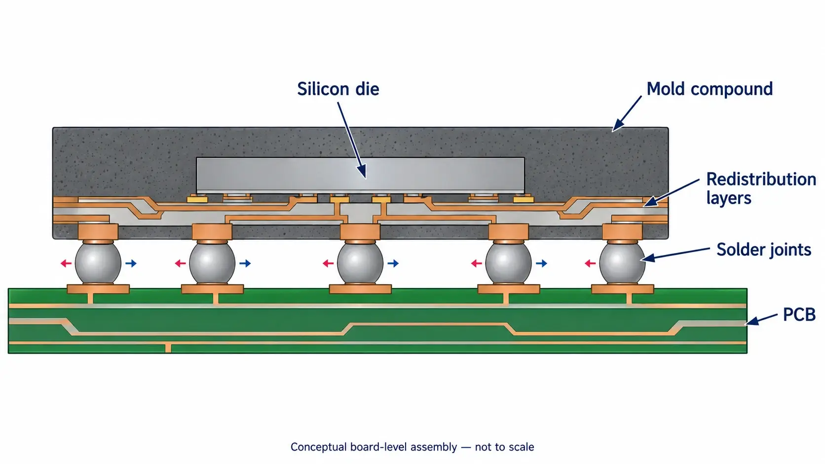
This conceptual section shows the board-level interface. It is not a DEEPETCH product drawing. The arrows indicate possible differential expansion, not a calculated displacement or a measured stress result.
Request the recommended land pattern, solder mask arrangement, paste and reflow guidance. Identify whether underfill or edge bonding is required, optional or unsuitable for the application. Adding a reinforcement material can change rework and inspection requirements, so it should be part of the qualified assembly process rather than an improvised repair for a failed trial.
The verification plan should reflect the product’s actual use. Temperature cycling, mechanical loading, moisture exposure and powered operation are not interchangeable tests. Specify the relevant conditions and failure criteria with the responsible package and reliability engineers. A compact consumer device and an industrial module may use a similar package outline but face different service conditions.
Wafer-scale processing can spread some operations across many devices. It does not remove mask costs, process development, test, handling loss or assembly fallout. Fan-out adds its own reconstruction and routing requirements. A low package price is not enough to choose a process.
Ask each quotation to separate one-time engineering charges from recurring unit costs. Check what is included in wafer preparation, bumping or RDL, inspection, electrical test, singulation and final packing. State who supplies the incoming wafers or dies and who bears the cost of rejected material.
For the board comparison, include any extra PCB layers, via requirements, assembly development and yield loss. Use the same forecast volume and acceptance criteria for both proposals. If these assumptions differ, the two prices are answering different questions.
DEEPETCH’s IDM customization services are a route for discussing the project scope. Before requesting a specific fan-out flow, confirm which operations, partners and qualification evidence are available for that design. A general packaging service description does not establish a production-qualified process for every WLP architecture.
A first review is more productive with these inputs:
If one item is still open, identify it as a decision to be resolved. For example, a flexible package outline may allow the engineer to trade a little area for easier board routing. Hiding that flexibility in an incomplete drawing makes the comparison harder.
No. Chip-scale describes a size relationship, while wafer-level describes how packaging operations are organized. A substrate-based FCCSP and a fan-in WLCSP can both be compact without sharing the same construction.
Some fan-out architectures use RDL and mold compound without a conventional laminate substrate in that package layer. Other assemblies combine fan-out structures with additional substrates or components. Ask for the full assembly cross-section before assuming the entire system is substrate-free.
The die-to-board connection problem comes first. If the ball map, routing, height and assembly requirements can be met with a qualified fan-in process, there may be little reason to add a fan-out flow. If connection area or integration requirements exceed that option, evaluate fan-out alongside a substrate-based design. Select the route that meets the complete specification with an acceptable qualification plan.
Send the drawings and unresolved constraints to DEEPETCH’s technical team for a scope review. The useful outcome is a defined package architecture, process responsibility and validation plan, not simply a quotation labeled “wafer level packaging.”

The DE-CW-1310 DFB EPI wafer, a high-performance epitaxial structure designed for distributed feedback (DFB) lasers operating at 1310 nm....

Ceramic thin-filmvacuum sensor Optical gas massflowmeter Liquid mass flowmeter Force sensor MEMS...

Photoelectric sensing chip Light source chips Optical transmission and modulationchips Optical detection and receptionchips...

Using a“Detach Core”which has two-layers carrier foil structure on the surface as a core, and forming...

Tenting process is a kind of subtractive process, the process as follows: Laminating photosensitive film...

Modified Semi-Added Process abbreviated as mSAP, which can be used on the core or build-up layers, pattern...

Semi-Added Process abbreviated as SAP, using on the build-up-layer pattern forming as follow:First depositing...

The product generally adopts the pressing lamination process of semi-curing sheets , and line formation...

The products generally adopt the Build-up Film Lamination process, and the circuit formation uses the...
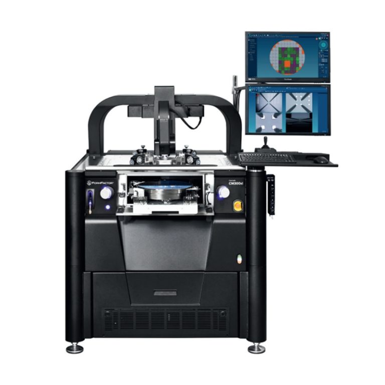
Equipment features: 1. Non-destructive precision testing Micrometer-level probe contact technology...