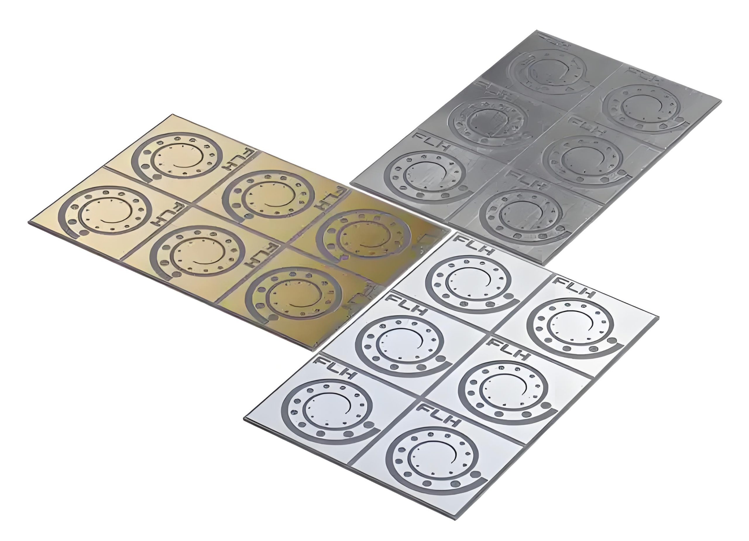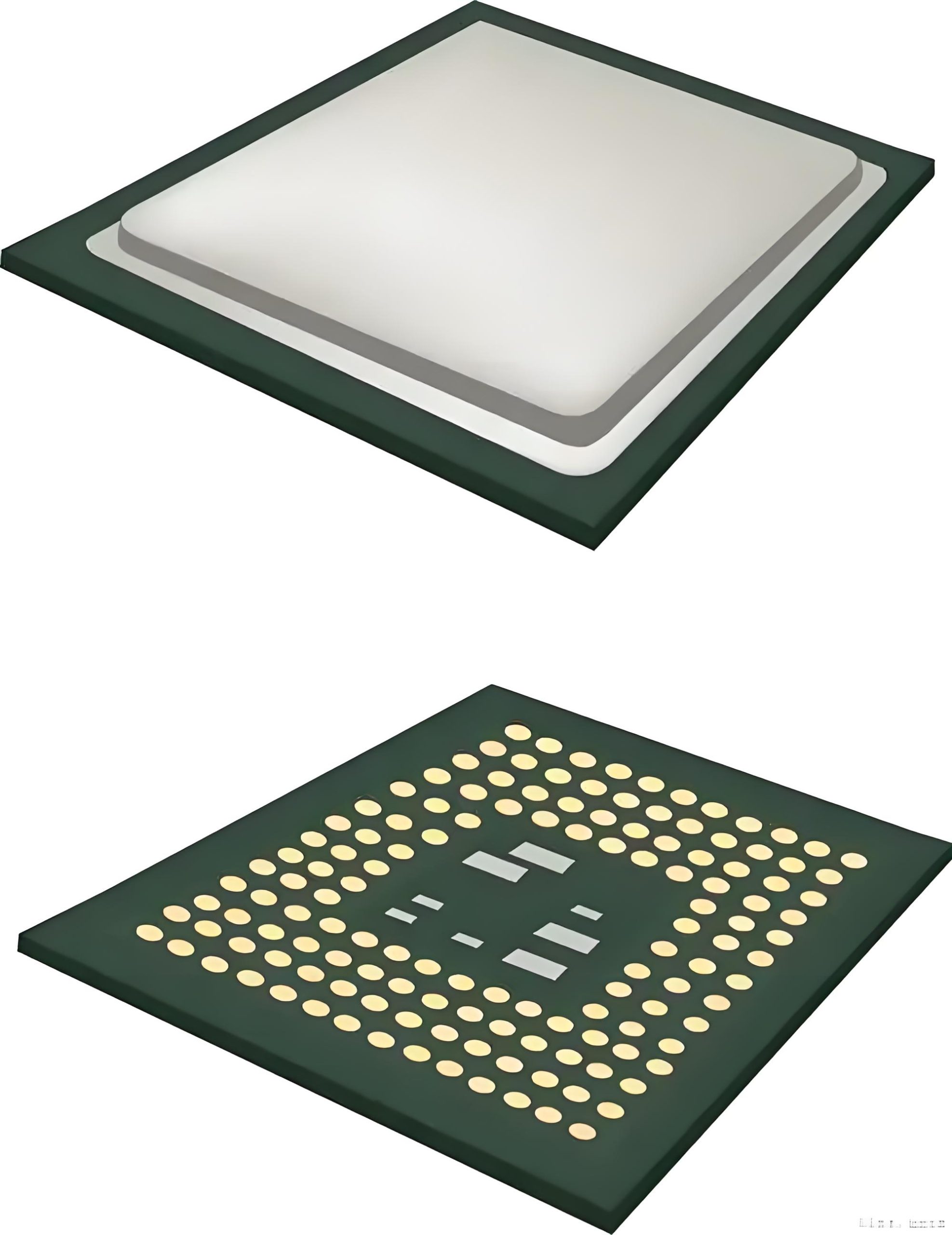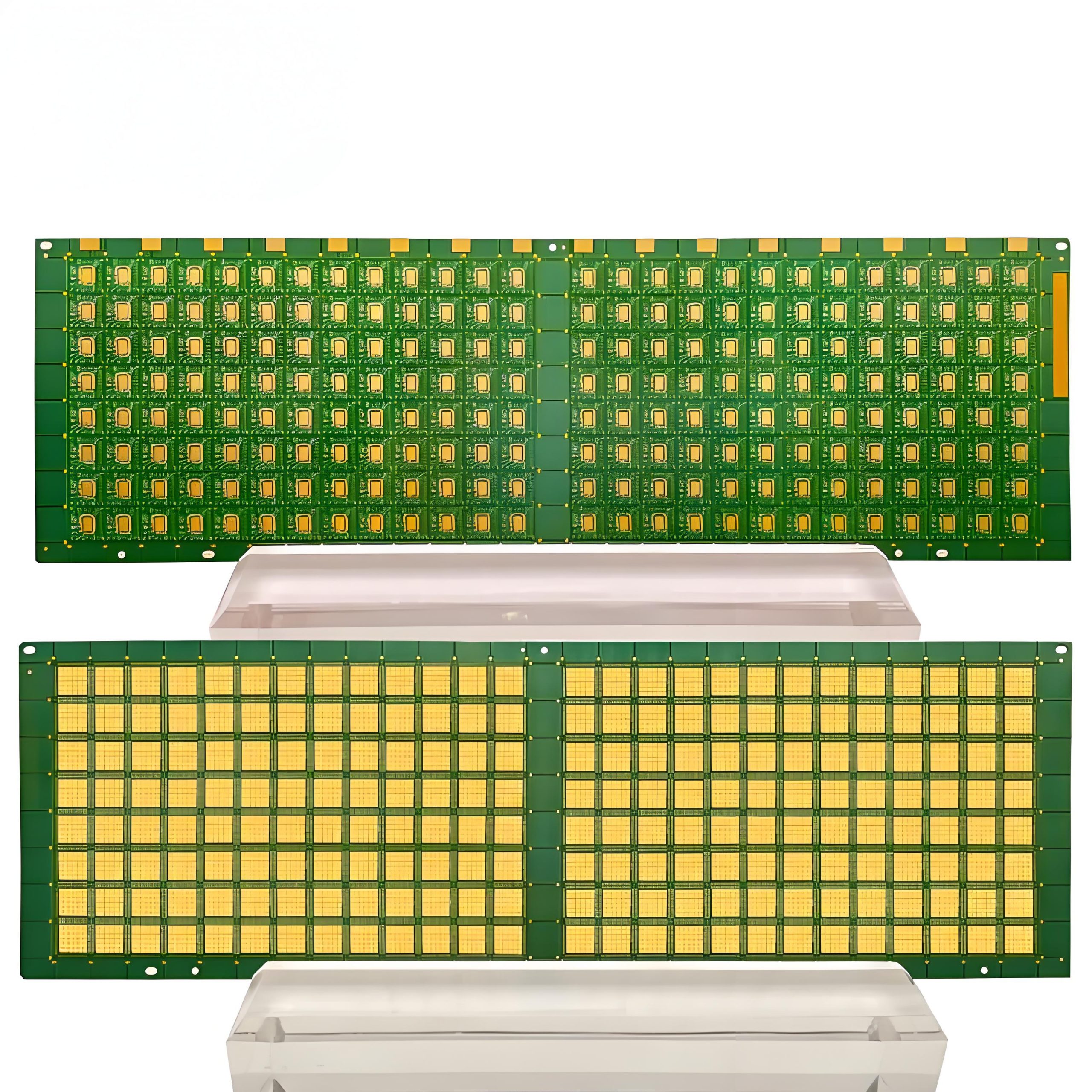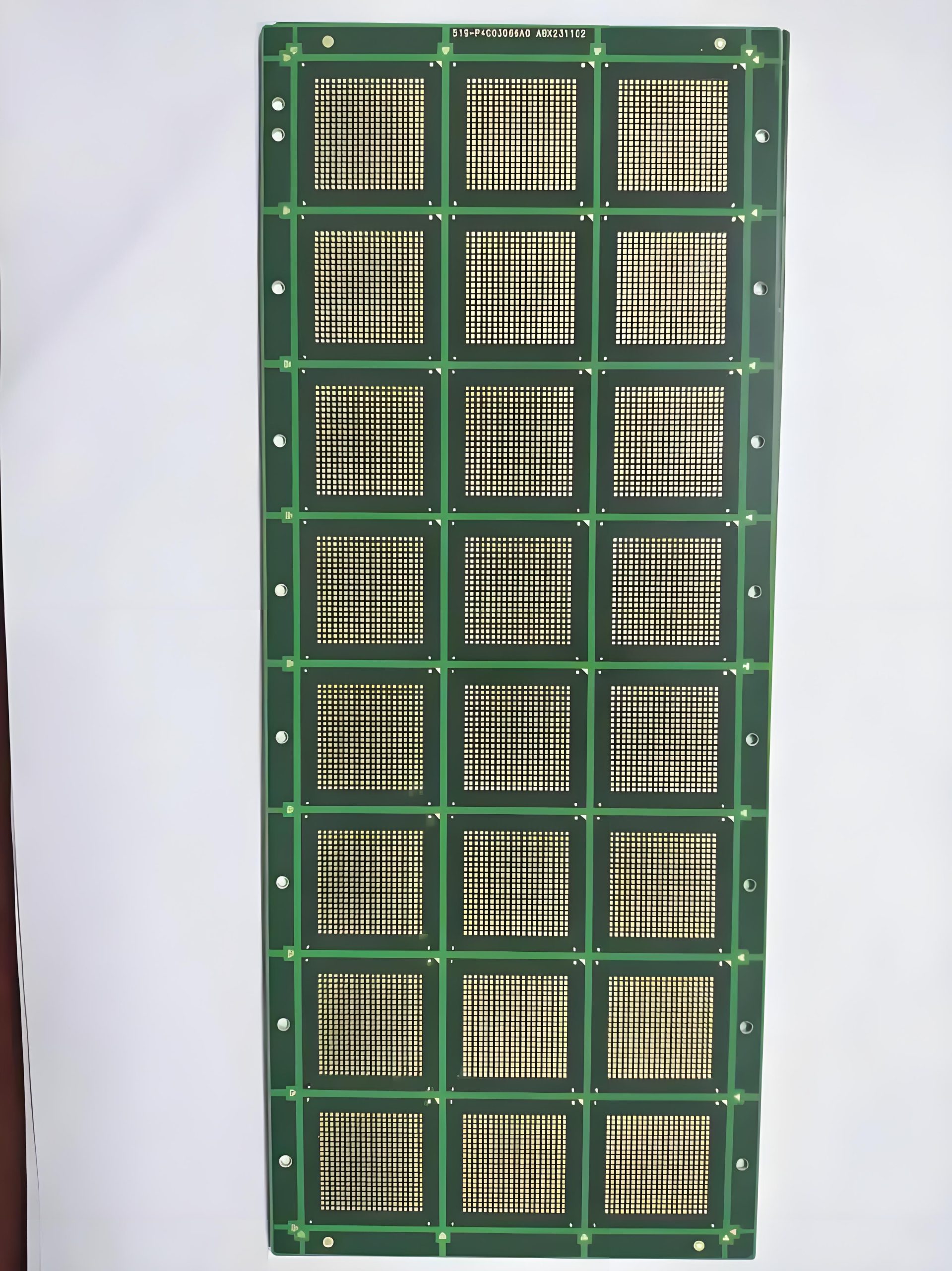


Copper Substrate

Product album display

Application Areas

  • High matching industries

New energy vehicles: 800V SIC inverter module (such as Tesla MODEL 3 rear drive module).

5G communication: MASSIVE MIMO AAU power amplifier (Huawei32T32R equipment).

Aerospace: Starborne phased array radar T/R components (temperature resistant-196℃ ~ +200℃).

Industrial power supply: 10KV/1000A IGBT crimping package.

  • Industry application and technical index advantages
  1. Power semiconductors (IGBT, SIC/GAN modules)

High thermal conductivity (>100 W/M·K) reduces junction temperature and improves device life; low CTE (6-8×10⁻⁶/K) matches SI/SIC chips and reduces thermal stress cracking. Suitable for electric vehicle inverters, industrial frequency converters, photovoltaic inverters.

  1. LED packaging (high power LED, COB packaging)

High efficiency heat dissipation, improve LED light efficiency and life, copper high reflectivity can improve LED light output efficiency, suitable for car headlights, outdoor display screens, plant lighting.

  1. RF/microwave devices (5G base stations, radar)

Low dielectric loss (DBC ceramic insulation layer), suitable for high frequency applications, copper’s high conductivity reduces signal loss, suitable for 5G PA module, military radar, satellite communication.

  1. Automotive electronics (electric drive, BMS, on-board charging)

High temperature resistance, vibration resistance, suitable for harsh vehicle environment, high current carrying capacity, suitable for high power electric drive system, suitable for electric vehicle motor controller, battery management system (BMS).


IDM Customization Service

From advanced processes to specialty processes, we use our IDM vertical integration experience to help customers overcome design-process collaboration challenges.

01

Supports advanced nodes such as [5-22nm FinFET/BCD/GAA] to meet the needs of high-performance computing (HPC), AI chips, etc.

02

MPW (Multi-Project Wafer) Service: Small batch trial production to reduce customers' initial costs. Customized process development: Cooperate with customers to conduct DTCO (Design-Process Co-Optimization), customize design rules and process parameters.

03

We support the joint solution of "wafer foundry + advanced packaging" (such as 3D IC, heterogeneous integration) to avoid the loss of multi-supplier collaboration. Unlike pure foundries, we verify the process stability through mass production of our own chips to reduce the risk of tape-out for you.

Provide customers with complete integrated manufacturing services from concept to finished product

01

Electronic manufacturing services and printed circuit board assembly.

02

EMS provides a wide range of electronic manufacturing services, including everything from circuit board design to supply chain management to assembly, testing and after-sales support.

03

PCBA is a link in EMS that focuses on the assembly of printed circuit boards, covering component placement, soldering and related testing, connecting electronic components to manufactured printed circuit boards.

News Center