
DAF/DDAF Die Attach Film

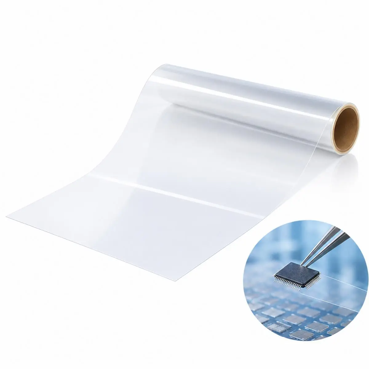
The SCH Series is a high-performance DAF/DDAF (Die Attach Film) designed to streamline and enhance the advanced packaging process. Applied to the wafer backside before dicing, this film serves a dual purpose: it secures the wafer during the cutting process and acts as a permanent adhesive layer to firmly bond the singulated chips to substrates or frames. Available in ultra-thin thicknesses of 10 to 50 μm, the SCH Series eliminates the need for liquid adhesives, ensuring uniform bond lines and high reliability for modern semiconductor packaging.

DAF/DDAF Die Attach Film

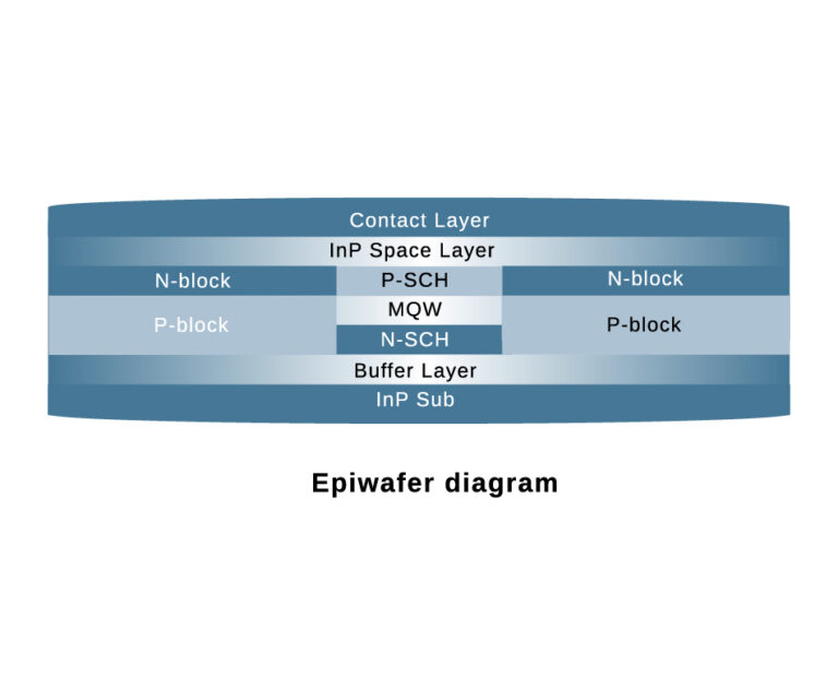
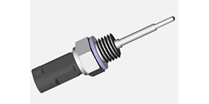
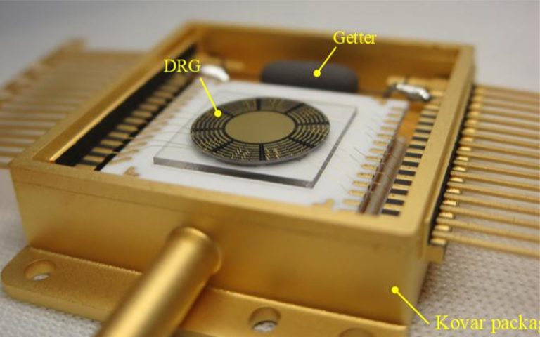
Product album display

Key Features

  • Integrated Dicing & Bonding: Functions simultaneously as a dicing tape and a permanent die attach adhesive, simplifying the packaging workflow.

  • Ultra-Thin Profile: Offers customizable thicknesses from 10 μm to 50 μm to accommodate miniaturized and high-density packaging designs.

  • Excellent Reliability: Features a moisture absorption rate of < 1%, preventing delamination and ensuring long-term stability.

  • Broad Material Compatibility: Specifically engineered for bonding Glass-to-Glass, Glass-to-ABS, Wafer-to-Glass, and Wafer-to-Substrate (SCH-20).

  • Tailored Thermal Properties: Available in different grades to match specific process requirements (SCH-10: Curing at 85°C, Tg 90°C; SCH-20: Curing at 110°C, Tg 120°C).


Product Structure

  1. Top Release Liner: Protective film layer.

  2. DAF Layer: The core die attach film providing structural adhesion.

  3. Bottom Release Liner: Protective film layer.


DAF/DDAF Die Attach Film Technical Specifications

Item SCH-10 SCH-20
Curing Condition 85 °C 110 °C
Mounting Temperature 60 ~ 90 °C 60 ~ 90 °C
Tg 90 °C 120 °C
Thickness 10 ~ 50 μm 10 ~ 50 μm
Storage Modulus (at 30°C) / 3,000 MPa
Moisture Absorption < 1 % < 1 %
Contact Materials Glass to Glass, Glass to ABS Glass to Glass, Wafer to Glass, Wafer to Substrate
chip

Application Areas

  • Die to Die: Stacking chips for 3D integration.

  • Die to Substrates: Bonding chips directly to package substrates.

  • Die to Die FOW (Fan-Out Wafer): High-density fan-out wafer-level packaging.

  • Suitable for advanced packaging applications requiring precise bond line thickness and zero voiding.

IDM Customization Service

From advanced processes to specialty processes, we use our IDM vertical integration experience to help customers overcome design-process collaboration challenges.

01

Supports advanced nodes such as [5-22nm FinFET/BCD/GAA] to meet the needs of high-performance computing (HPC), AI chips, etc.

02

MPW (Multi-Project Wafer) Service: Small batch trial production to reduce customers' initial costs. Customized process development: Cooperate with customers to conduct DTCO (Design-Process Co-Optimization), customize design rules and process parameters.

03

We support the joint solution of "wafer foundry + advanced packaging" (such as 3D IC, heterogeneous integration) to avoid the loss of multi-supplier collaboration. Unlike pure foundries, we verify the process stability through mass production of our own chips to reduce the risk of tape-out for you.

Provide customers with complete integrated manufacturing services from concept to finished product

01

Electronic manufacturing services and printed circuit board assembly.

02

EMS provides a wide range of electronic manufacturing services, including everything from circuit board design to supply chain management to assembly, testing and after-sales support.

03

PCBA is a link in EMS that focuses on the assembly of printed circuit boards, covering component placement, soldering and related testing, connecting electronic components to manufactured printed circuit boards.

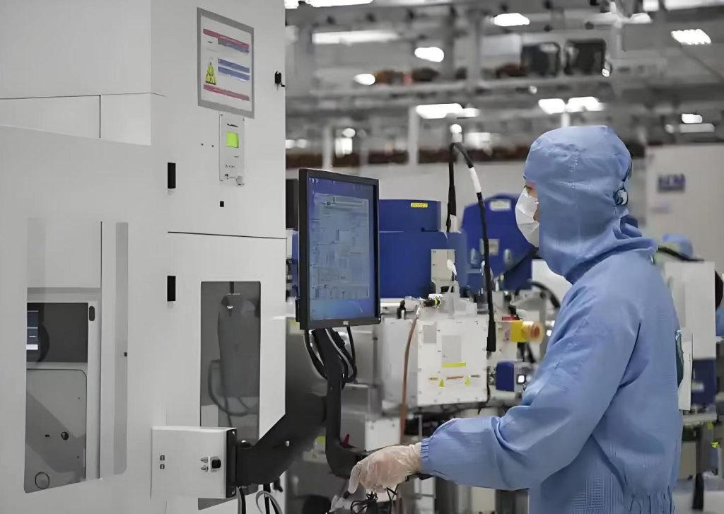
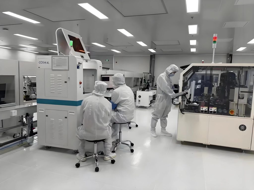
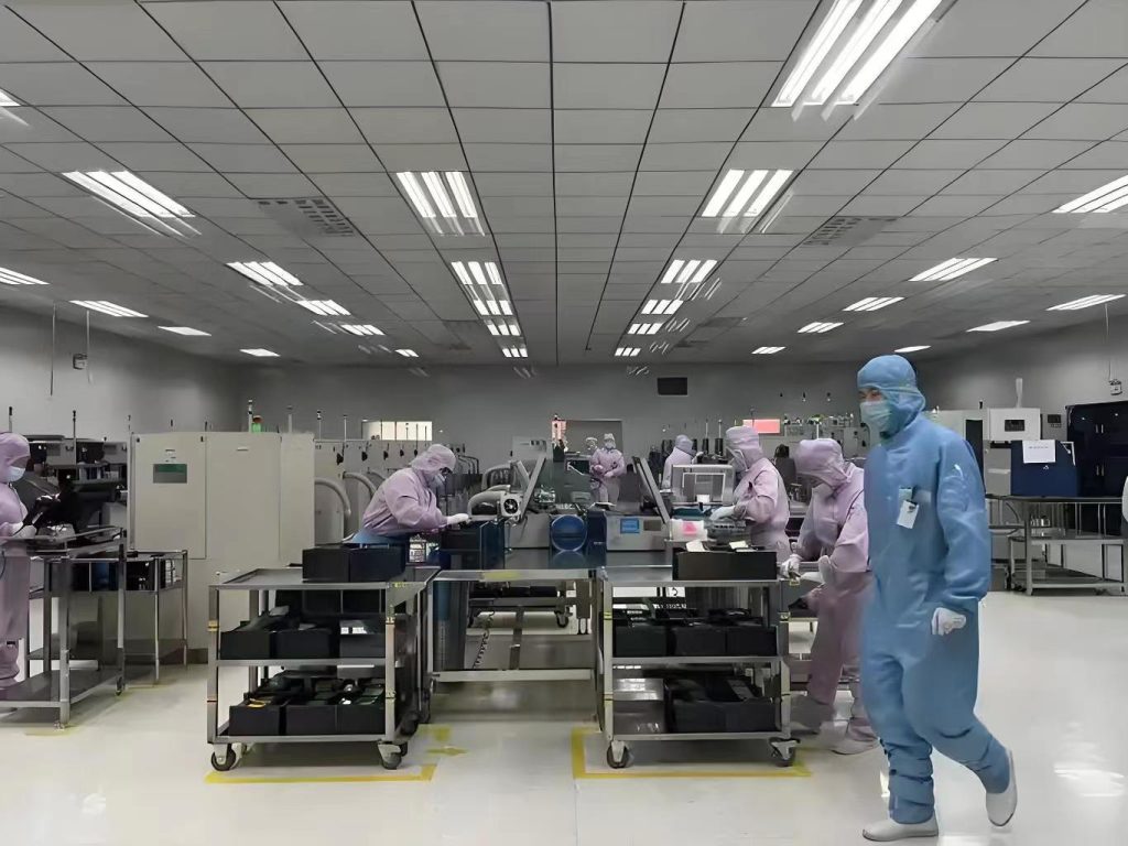
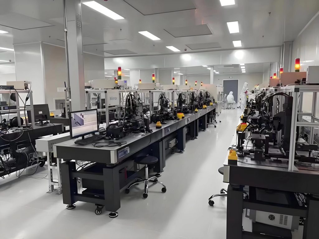
Semiconductor production shop environment

News Center