

High matching industries
Advantages: high toughness, biological inertness, avoid the rejection reaction of traditional metal implants.
Indicators: artificial hip joint life>20 years, crown bending strength>1200 MPA.
Advantages: temperature resistance> 800℃ (oxidation environment), suitable for engine oxygen sensor, high temperature probe.
Case: Automotive exhaust oxygen sensor (ZRO₂ based electrolyte), response time <50 MS.
Advantages: high hardness (Moissan hardness 8.5) and aesthetic, used in mobile phone backplane, smart wearable devices.
Indicator: 40% improvement in anti-fall performance (compared to glass backplane).
Advantages: low thermal expansion coefficient is close to that of metal, used in optical fiber connectors and bearing components.
Case: Ceramic bearings in semiconductor equipment, life extended by three times.
Advantages: resistant to corrosion by molten metals (such as aluminum, copper), used in electrolytic cell lining, fuel cell separator.
Diamond-Copper Thermally Conductive Composite. High thermal conductivity, tunable CTE, robust.

The DE-CW-1310 DFB EPI wafer, a high-performance epitaxial structure designed for distributed feedback (DFB) lasers operating at 1310 nm....

Ceramic thin-filmvacuum sensor Optical gas massflowmeter Liquid mass flowmeter Force sensor MEMS...

Photoelectric sensing chip Light source chips Optical transmission and modulationchips Optical detection and receptionchips...

Using a“Detach Core”which has two-layers carrier foil structure on the surface as a core, and forming...

Tenting process is a kind of subtractive process, the process as follows: Laminating photosensitive film...

Modified Semi-Added Process abbreviated as mSAP, which can be used on the core or build-up layers, pattern...

Semi-Added Process abbreviated as SAP, using on the build-up-layer pattern forming as follow:First depositing...

The product generally adopts the pressing lamination process of semi-curing sheets , and line formation...

The products generally adopt the Build-up Film Lamination process, and the circuit formation uses the...
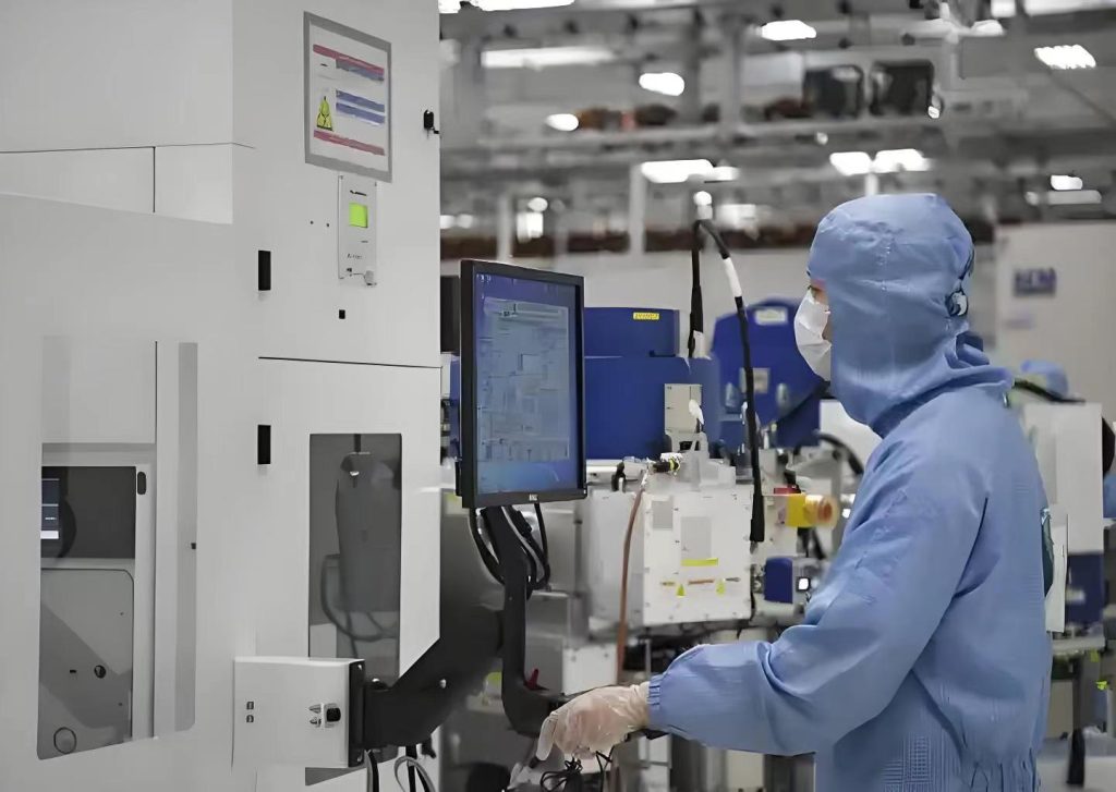
Supports advanced nodes such as [5-22nm FinFET/BCD/GAA] to meet the needs of high-performance computing (HPC), AI chips, etc.
MPW (Multi-Project Wafer) Service: Small batch trial production to reduce customers' initial costs. Customized process development: Cooperate with customers to conduct DTCO (Design-Process Co-Optimization), customize design rules and process parameters.
We support the joint solution of "wafer foundry + advanced packaging" (such as 3D IC, heterogeneous integration) to avoid the loss of multi-supplier collaboration. Unlike pure foundries, we verify the process stability through mass production of our own chips to reduce the risk of tape-out for you.
Electronic manufacturing services and printed circuit board assembly.
EMS provides a wide range of electronic manufacturing services, including everything from circuit board design to supply chain management to assembly, testing and after-sales support.
PCBA is a link in EMS that focuses on the assembly of printed circuit boards, covering component placement, soldering and related testing, connecting electronic components to manufactured printed circuit boards.
Title: Semiconductor manufacturing processes Objective: To have a certain foundation for the overall...