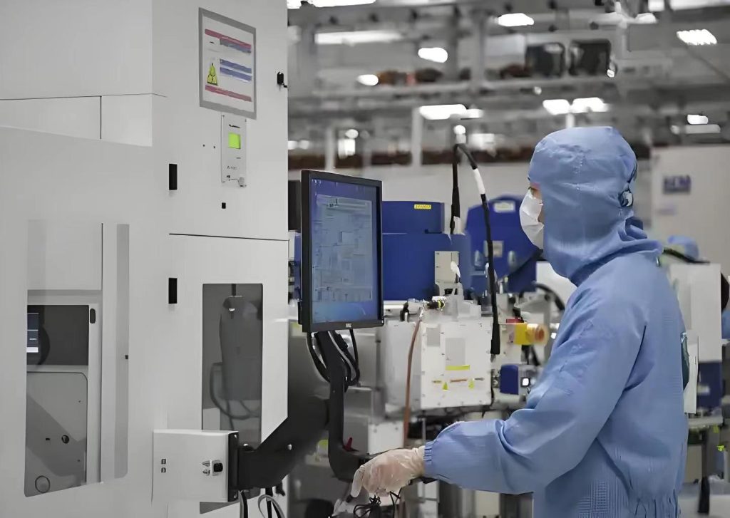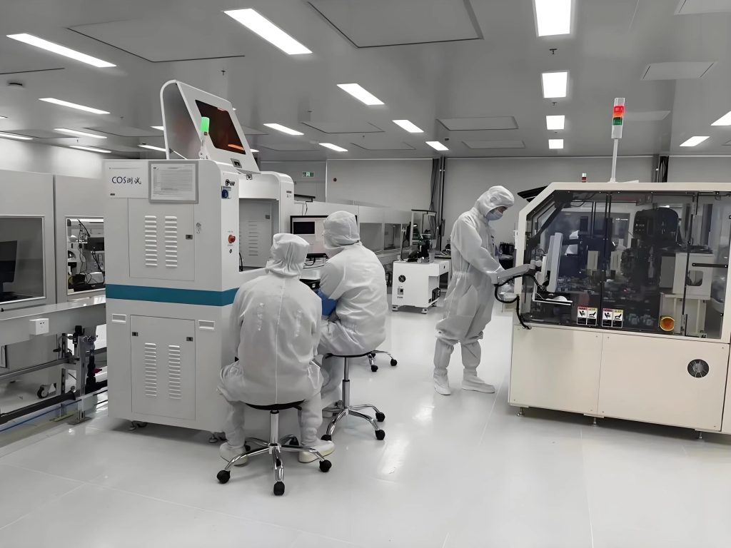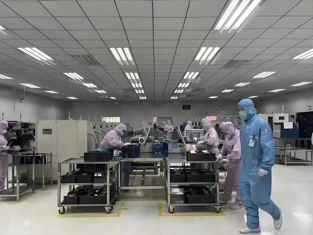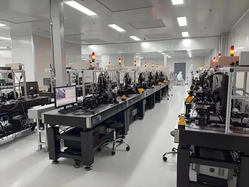


Silicon And Germanium (SiGe)

Product album display

Application Areas

Industry applications

  1. High frequency electronic devices

SIGE HBT (heterojunction bipolar transistor): used in power amplifiers (PA) for 5G base stations and radar to achieve high gain (>20 DB) and low noise (noise factor <1 DB).

RF CMOS Integration: Combining silicon and germanium with complementary metal oxide semiconductor (CMOS) to improve the performance of radio frequency integrated circuits (RFIC).

  1. Photoelectric devices

GE/SIGE Photoelectric Detector: A high-speed response (> 10 GB/S) is achieved in optical fiber communication (1.3-1.55ΜM band) for the absorber layer of the photoelectric detector.

Optical communication: Silicon-germanium photodetectors are used in optical modules for data centers to improve data transmission rates (e.g., 400G/800G)

Silicon-based laser: an epitaxial layer for a laser that uses the SIGE/SI quantum well structure to break through the indirect band gap of silicon and emit light.

  1. Stress silicon technology

High performance logic chips: Introduce SIGE stress layer in FINFET or nanosheet transistors to improve carrier mobility and switching speed (such as INTEL 14NM process).

  1. Artificial intelligence and edge computing

AI Chip: The high frequency and low power consumption characteristics of SIGE are suitable for the signal processing requirements of AI accelerator, which is suitable for real-time decision-making systems of autonomous driving and intelligent terminals.

Sensors: Short wave infrared (SWIR) sensors use SIGE epitaxial layers to enhance the environmental perception accuracy of autonomous vehicles


IDM Customization Service

From advanced processes to specialty processes, we use our IDM vertical integration experience to help customers overcome design-process collaboration challenges.

01

Supports advanced nodes such as [5-22nm FinFET/BCD/GAA] to meet the needs of high-performance computing (HPC), AI chips, etc.

02

MPW (Multi-Project Wafer) Service: Small batch trial production to reduce customers' initial costs. Customized process development: Cooperate with customers to conduct DTCO (Design-Process Co-Optimization), customize design rules and process parameters.

03

We support the joint solution of "wafer foundry + advanced packaging" (such as 3D IC, heterogeneous integration) to avoid the loss of multi-supplier collaboration. Unlike pure foundries, we verify the process stability through mass production of our own chips to reduce the risk of tape-out for you.

Provide customers with complete integrated manufacturing services from concept to finished product

01

Electronic manufacturing services and printed circuit board assembly.

02

EMS provides a wide range of electronic manufacturing services, including everything from circuit board design to supply chain management to assembly, testing and after-sales support.

03

PCBA is a link in EMS that focuses on the assembly of printed circuit boards, covering component placement, soldering and related testing, connecting electronic components to manufactured printed circuit boards.

News Center