

Silicon On Insulators (Soi)

products51

Product album display

chip

Application Areas

  • SOI’s industry applications
  1. High voltage and power devices

IGBT and MOSFET: buried oxygen layer isolation for high voltage (>1200 V) and reduced on-state resistance.

Automotive electronics: used in engine control units (ECUs) and battery management systems (BMS), with tolerance to extreme temperatures of-40℃ to 150℃.

  1. RF and microwave devices

Radio frequency front end (RF-SOI): Used for 5G millimeter wave RF switches (such as SKYWORKS’S SKY5® series), insertion loss <0.5 DB

5G chip: SOI’s low parasitic capacitance and high cutoff frequency (FT>200 GHZ) improve signal transmission efficiency.

Millimeter wave radar: used for 77 GHZ vehicle-mounted radar chip to reduce signal loss.

Low-power processors: IBM’s POWER server chips use SOI technology to improve energy efficiency by 40%

  1. Sensor MEMS

Pressure sensor: the insulation of the buried oxygen layer is used to achieve high sensitivity and anti-interference ability.

Micro accelerometer: The mechanical stability of SOI supports high precision inertial measurement.

Gyro: SOI technology is used in MEMS gyroscopes to improve accuracy and stability

  1. Anti-radiation electronic equipment

Aerospace: The buried oxygen layer reduces the charge accumulation caused by ionizing radiation and improves the ability to resist single particle flip (SEU).

  1. High performance integrated circuits

Microprocessors: SOI technology is used in high-performance microprocessors to improve speed and reduce power consumption.

Quantum bits: Spin quantum bits of silicon in SOI structure, with decoherence time extended to more than 1 second

IDM Customization Service

From advanced processes to specialty processes, we use our IDM vertical integration experience to help customers overcome design-process collaboration challenges.

01

Supports advanced nodes such as [5-22nm FinFET/BCD/GAA] to meet the needs of high-performance computing (HPC), AI chips, etc.

02

MPW (Multi-Project Wafer) Service: Small batch trial production to reduce customers' initial costs. Customized process development: Cooperate with customers to conduct DTCO (Design-Process Co-Optimization), customize design rules and process parameters.

03

We support the joint solution of "wafer foundry + advanced packaging" (such as 3D IC, heterogeneous integration) to avoid the loss of multi-supplier collaboration. Unlike pure foundries, we verify the process stability through mass production of our own chips to reduce the risk of tape-out for you.

Provide customers with complete integrated manufacturing services from concept to finished product

01

Electronic manufacturing services and printed circuit board assembly.

02

EMS provides a wide range of electronic manufacturing services, including everything from circuit board design to supply chain management to assembly, testing and after-sales support.

03

PCBA is a link in EMS that focuses on the assembly of printed circuit boards, covering component placement, soldering and related testing, connecting electronic components to manufactured printed circuit boards.

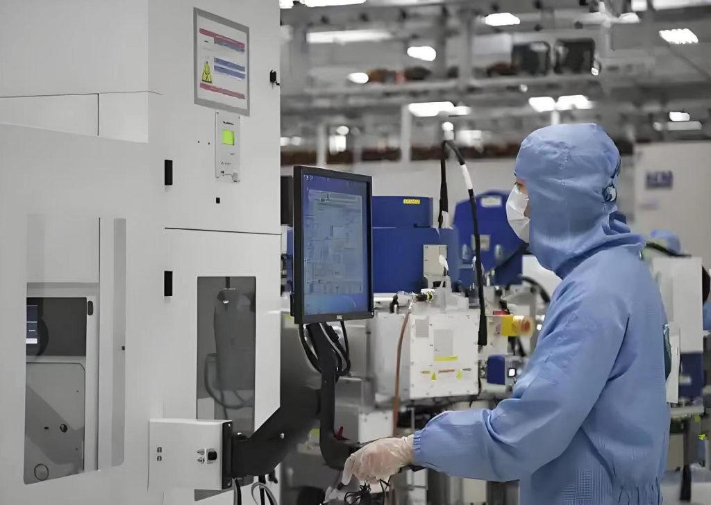
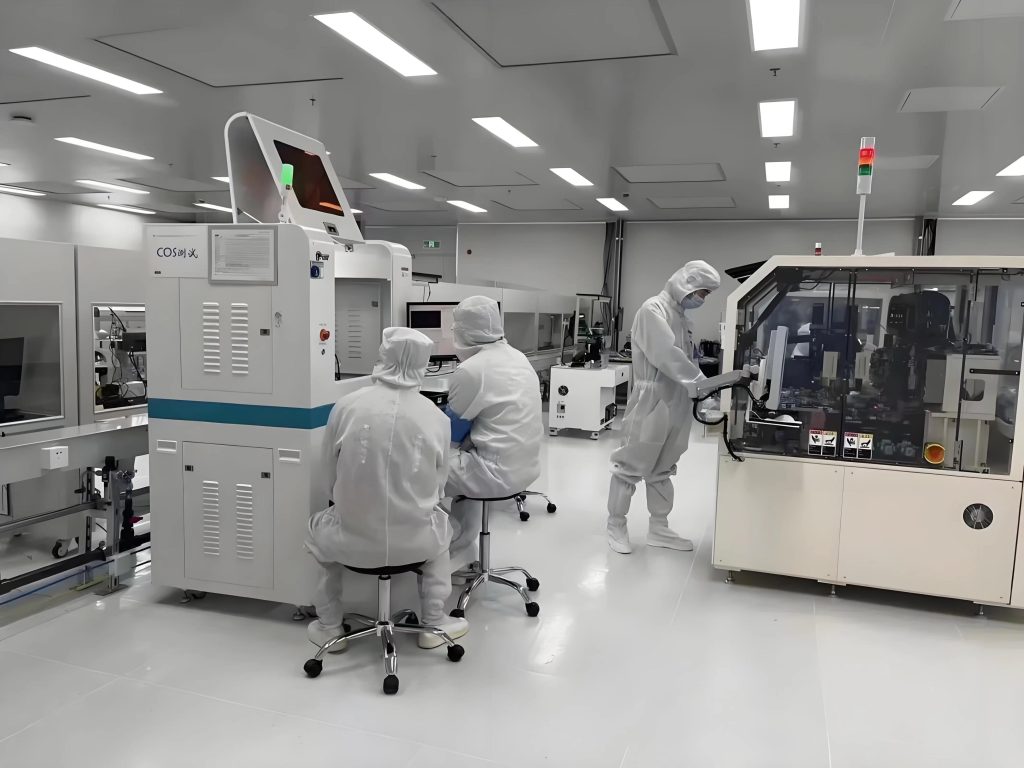
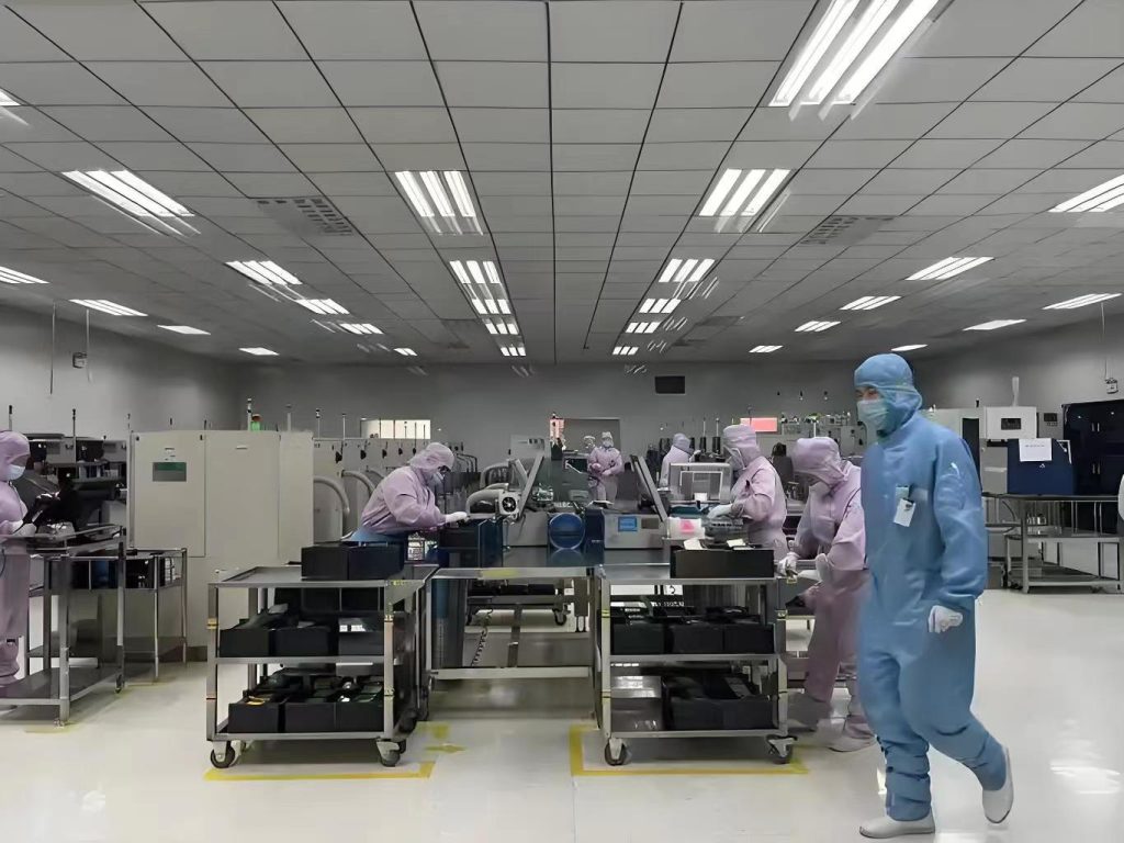
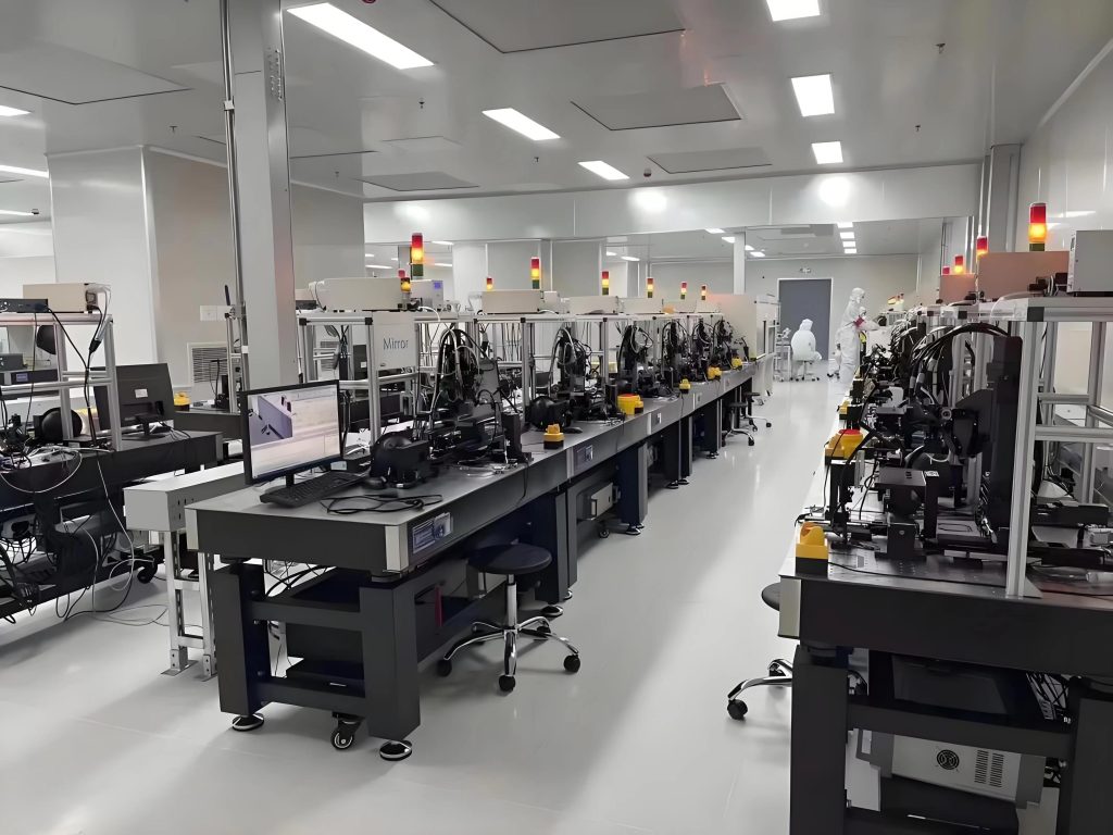
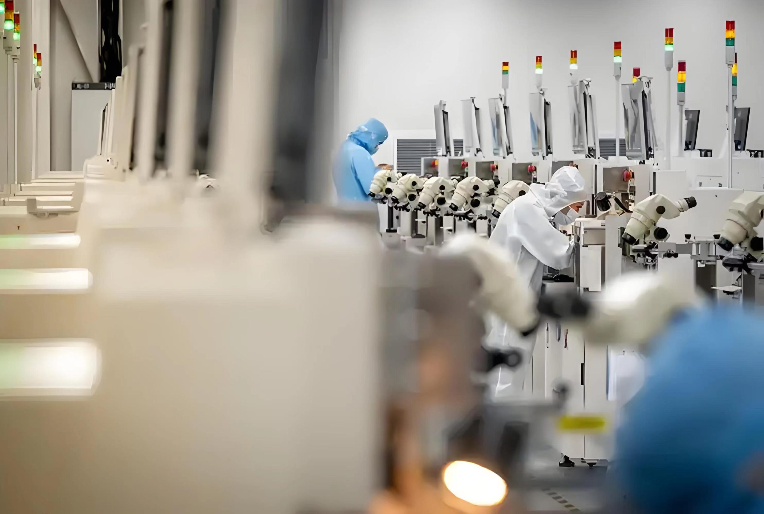
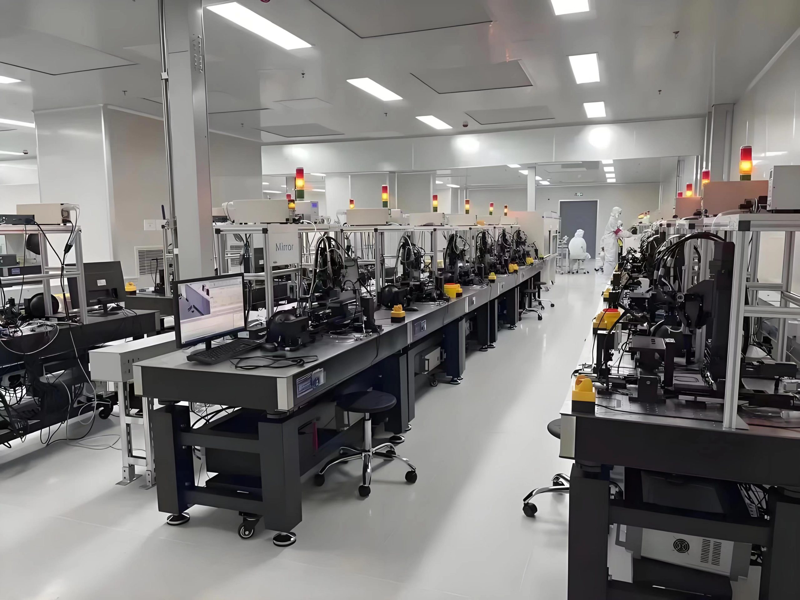
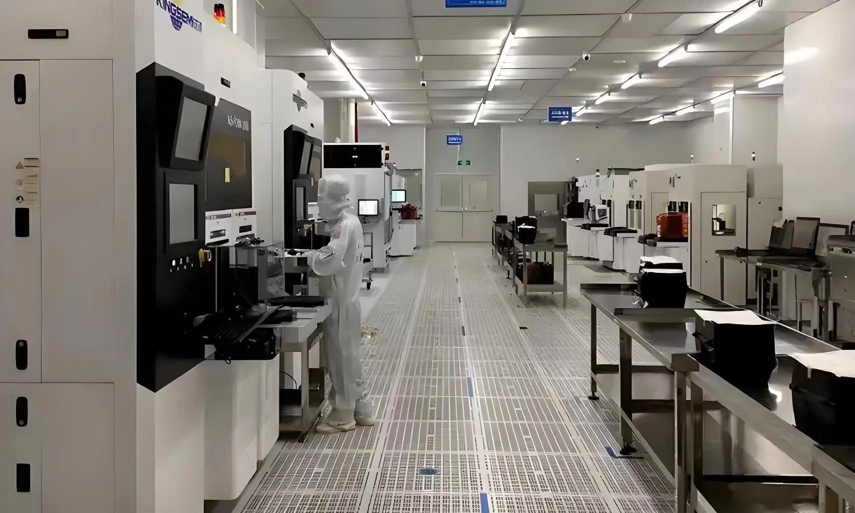
Semiconductor production shop environment

News Center