
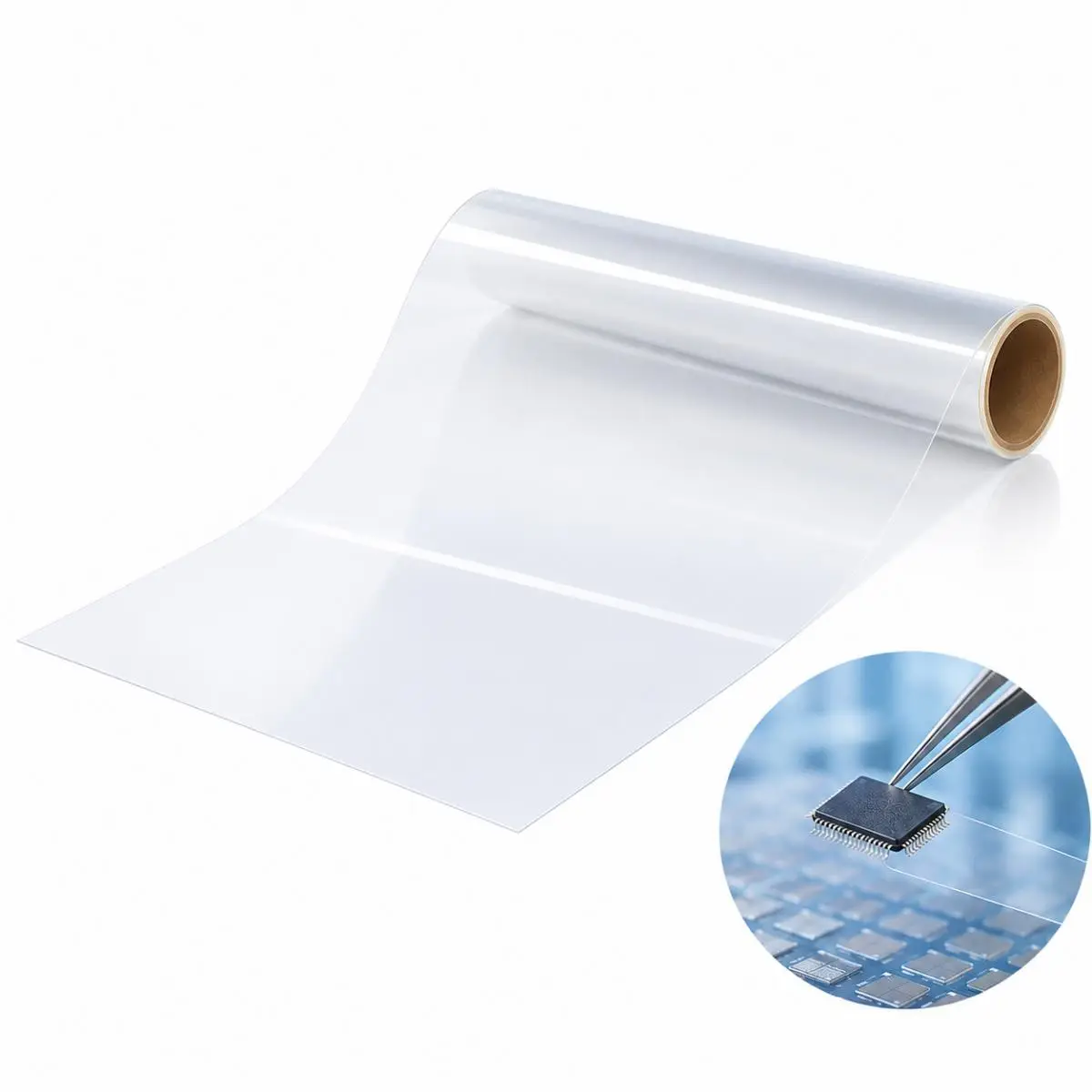
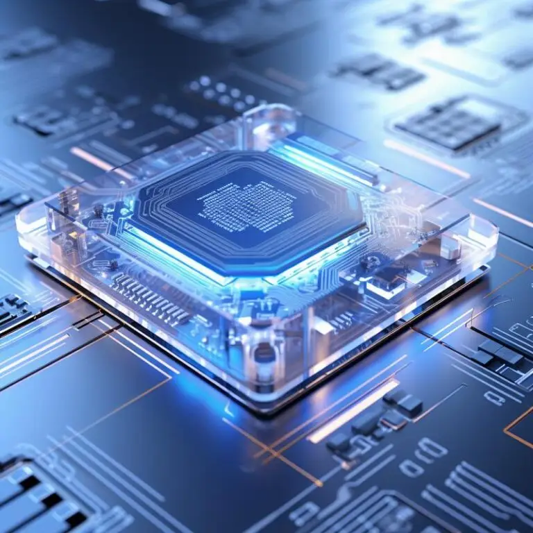
The SCH Series is a high-performance DAF/DDAF (Die Attach Film) designed to streamline and enhance the advanced packaging process. Applied to the wafer backside before dicing, this film serves a dual purpose: it secures the wafer during the cutting process and acts as a permanent adhesive layer to firmly bond the singulated chips to substrates or frames. Available in ultra-thin thicknesses of 10 to 50 μm, the SCH Series eliminates the need for liquid adhesives, ensuring uniform bond lines and high reliability for modern semiconductor packaging.
Integrated Dicing & Bonding: Functions simultaneously as a dicing tape and a permanent die attach adhesive, simplifying the packaging workflow.
Ultra-Thin Profile: Offers customizable thicknesses from 10 μm to 50 μm to accommodate miniaturized and high-density packaging designs.
Excellent Reliability: Features a moisture absorption rate of < 1%, preventing delamination and ensuring long-term stability.
Broad Material Compatibility: Specifically engineered for bonding Glass-to-Glass, Glass-to-ABS, Wafer-to-Glass, and Wafer-to-Substrate (SCH-20).
Tailored Thermal Properties: Available in different grades to match specific process requirements (SCH-10: Curing at 85°C, Tg 90°C; SCH-20: Curing at 110°C, Tg 120°C).
Top Release Liner: Protective film layer.
DAF Layer: The core die attach film providing structural adhesion.
Bottom Release Liner: Protective film layer.
| Item | SCH-10 | SCH-20 |
|---|---|---|
| Curing Condition | 85 °C | 110 °C |
| Mounting Temperature | 60 ~ 90 °C | 60 ~ 90 °C |
| Tg | 90 °C | 120 °C |
| Thickness | 10 ~ 50 μm | 10 ~ 50 μm |
| Storage Modulus (at 30°C) | / | 3,000 MPa |
| Moisture Absorption | < 1 % | < 1 % |
| Contact Materials | Glass to Glass, Glass to ABS | Glass to Glass, Wafer to Glass, Wafer to Substrate |
Die to Die: Stacking chips for 3D integration.
Die to Substrates: Bonding chips directly to package substrates.
Die to Die FOW (Fan-Out Wafer): High-density fan-out wafer-level packaging.
Suitable for advanced packaging applications requiring precise bond line thickness and zero voiding.
The SCH Series is a high-performance DAF/DDAF (Die Attach Film) designed to streamline and enhance the advanced packaging process....
The DEEPETCH DP-QPA2611 is a high-performance X-Band (8–12 GHz) Gallium Nitride (GaN) Power Amplifier...
The DEEPETCH DP-ROS-40121 is a premium, solvent-free epoxy die attach adhesive engineered for the most...
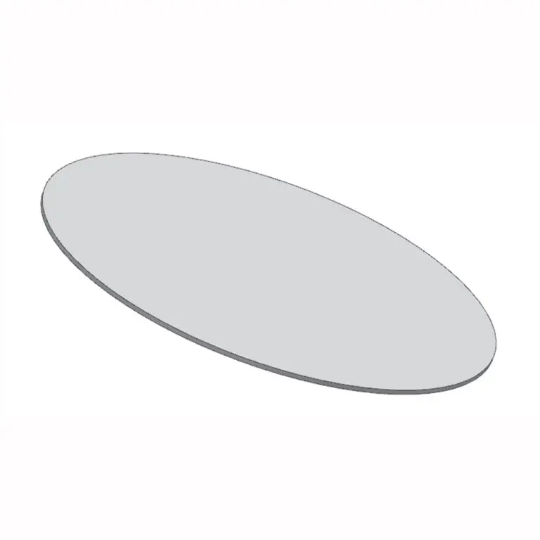
The Diamond Heat Spreader is a highly efficient thermal management material engineered for the most demanding...
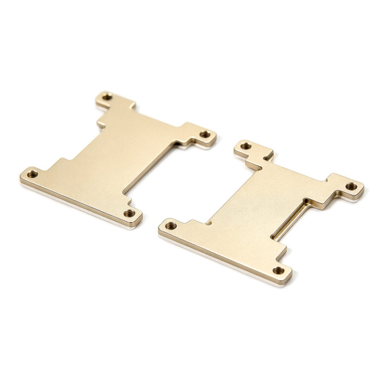
Molybdenum copper composite: adjustable CTE, high conductivity, lower density than tungsten copper. No...
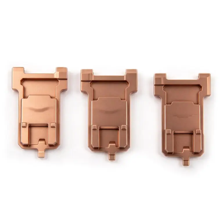
Tungsten copper composite: low CTE, high conductivity. Ideal for RF, power, optical packaging.
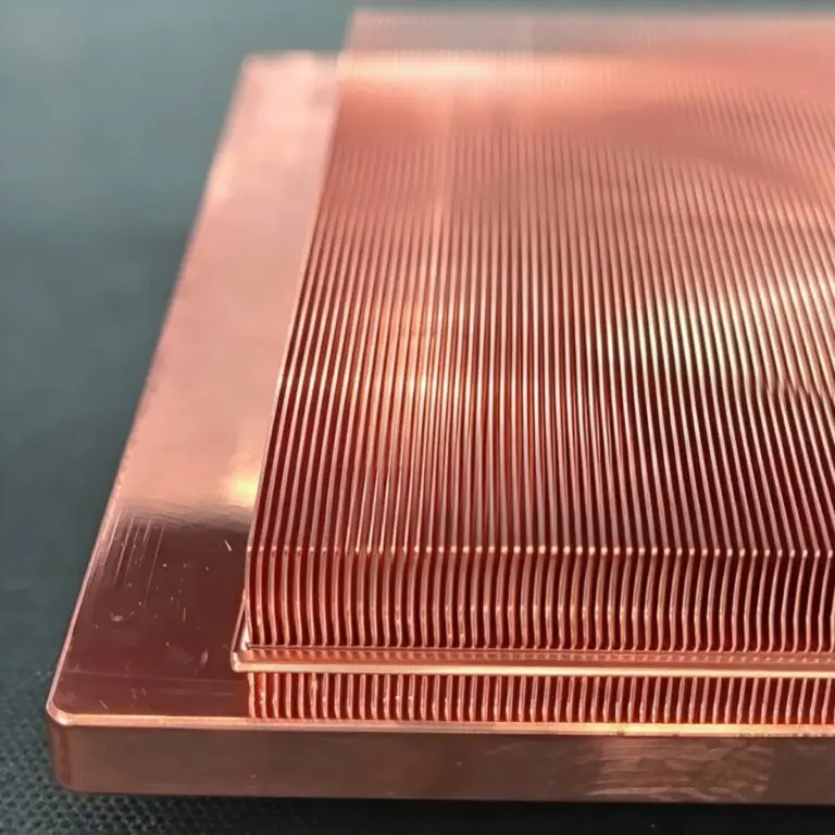
Diamond-Copper Thermally Conductive Composite. High thermal conductivity, tunable CTE, robust.
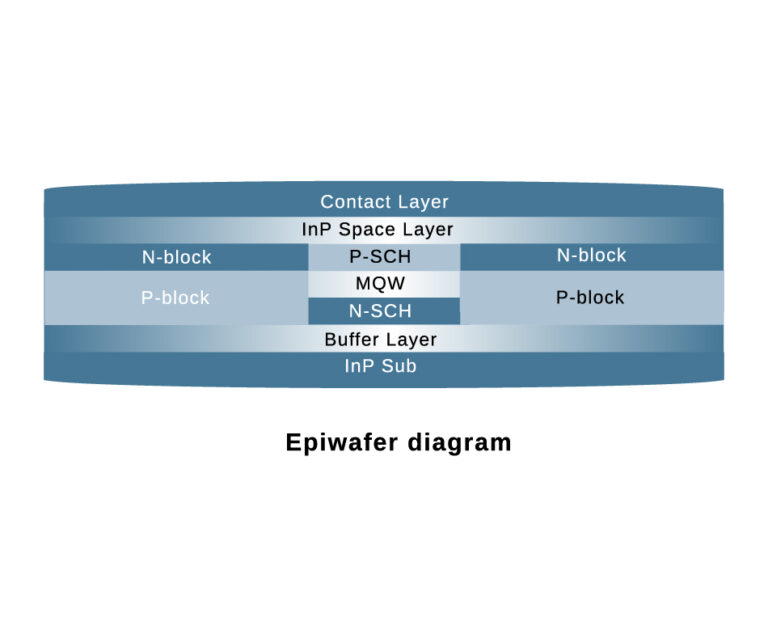
The DE-CW-1310 DFB EPI wafer, a high-performance epitaxial structure designed for distributed feedback (DFB) lasers operating at 1310 nm....
Ceramic thin-filmvacuum sensor Optical gas massflowmeter Liquid mass flowmeter Force sensor MEMS...
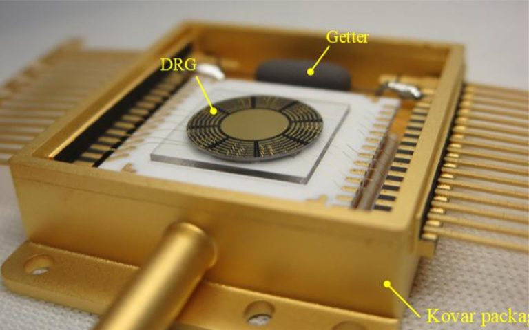
Photoelectric sensing chip Light source chips Optical transmission and modulationchips Optical detection and receptionchips...
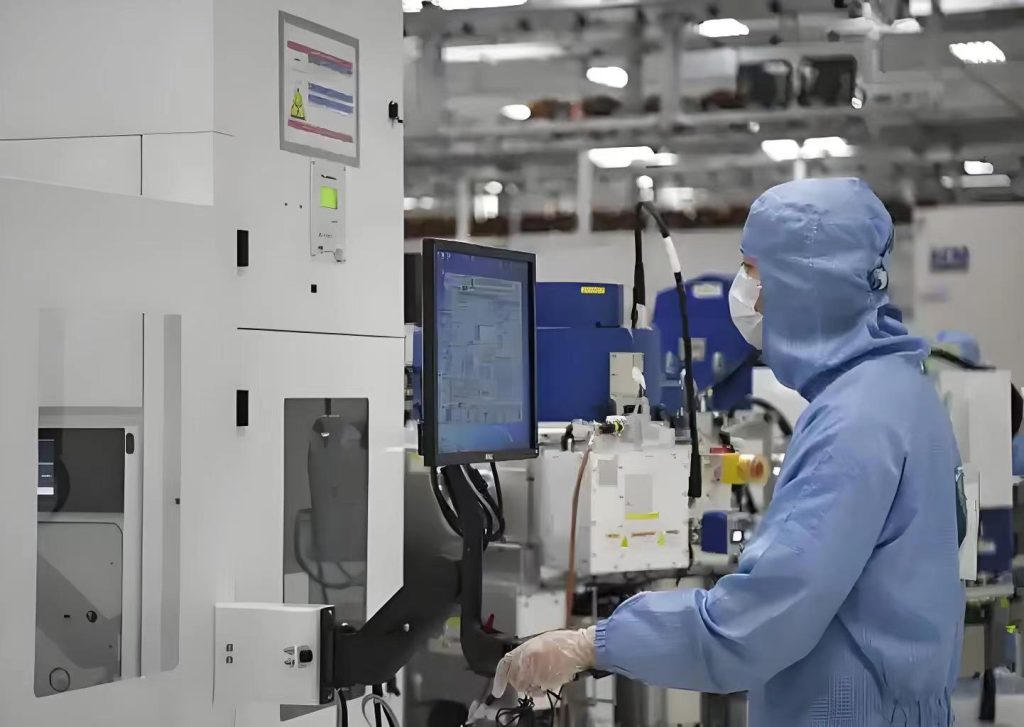
Supports advanced nodes such as [5-22nm FinFET/BCD/GAA] to meet the needs of high-performance computing (HPC), AI chips, etc.
MPW (Multi-Project Wafer) Service: Small batch trial production to reduce customers' initial costs. Customized process development: Cooperate with customers to conduct DTCO (Design-Process Co-Optimization), customize design rules and process parameters.
We support the joint solution of "wafer foundry + advanced packaging" (such as 3D IC, heterogeneous integration) to avoid the loss of multi-supplier collaboration. Unlike pure foundries, we verify the process stability through mass production of our own chips to reduce the risk of tape-out for you.
Electronic manufacturing services and printed circuit board assembly.
EMS provides a wide range of electronic manufacturing services, including everything from circuit board design to supply chain management to assembly, testing and after-sales support.
PCBA is a link in EMS that focuses on the assembly of printed circuit boards, covering component placement, soldering and related testing, connecting electronic components to manufactured printed circuit boards.
Title: Semiconductor manufacturing processes Objective: To have a certain foundation for the overall...