

“Add diamond” is not a thermal design. It leaves out the hotspot, the interfaces and even the face that will be joined. A diamond heat spreader makes sense where a small, hot region must feed a much larger cooling surface. That pattern now appears in AI accelerators and HBM packages, as well as RF and laser devices. DEEPETCH supplies diamond materials for this part of the package. The useful enquiry, though, starts with the stack—not with the highest number in a material table.
A cold plate can be working properly while the junction stays too hot. The restriction may be lower down: a narrow die contact, an uneven attachment layer, or too little room for heat to spread before it reaches the lid. Changing the liquid loop will not correct those faults.
Sketch a section through the package. Where is the heat made? How wide is that source? Now follow the path through the attach layer, spreader, lid and next interface. The sketch will show whether heat mainly travels straight through or first has to move sideways.
That distinction gives a diamond heat spreader for AI chips a specific job. It enlarges the active path near the die; the heatsink or cold plate still removes the heat afterward. If the contact below the diamond is poor, impressive bulk conductivity will not rescue the assembly.
“Near the die” is not precise enough. The part may sit below the die, above it, beneath a lid or inside a frame. Each location changes the useful footprint and the face that must be prepared for joining. It also changes what receiving can inspect.
Mark the growth face and nucleation face on the drawing. Name the joining side. If the surrounding frame controls an edge or datum, show that too. A CVD diamond heat spreader can be polished and metallized, but the supplier should not have to guess which surface meets the device.
Thermal conductivity is a screening value, not a junction-temperature promise. The assembled result also depends on thickness, area and contact. A slightly lower grade in good contact may do more useful work than a headline grade placed behind a weak interface.
The DEEPETCH diamond thermal product range is listed at 800–2000 W/m·K, with density of 3.51 g/cm³. CTE at 300 K is listed as 1.0 ± 0.1 ppm/K. These are sensible starting inputs for a package model. They are not a substitute for that model.
Geometry may settle the first decision. DEEPETCH lists single-crystal sizes up to 25 × 25 mm and polycrystalline sizes up to 50 mm. The standard thickness shown is 300 μm; custom dimensions are available. For a diamond heat spreader for AI chips, ask two plain questions. Can one piece cover the required spreading area? Will the selected thickness fit without moving another critical surface?
Diamond heat spreader thermal conductivity varies across the offered range. Put the required value or grade on the drawing only after the model identifies what is actually needed. Ordering the maximum by habit can narrow supply without improving the package.
The published face data are different. DEEPETCH lists roughness below 100 nm Ra on the growth side and below 30 nm Ra on the nucleation side. Parallelism is listed below 4 μm/cm. Those fields belong beside the face callout, not in an email that receiving may never see.
Titanium and gold coatings are available. Diamond heat spreader metallization needs its own order line: coated face, coverage and any edge clearance. If a bondable patch or patterned area is required, attach the drawing. The later soldering, brazing or other joining step should decide the coating sequence.
A material certificate answers a narrow question: what was supplied? The device team has another one: what happened after assembly? That is why a bare coupon result cannot close package qualification.
Attach thickness matters. So do voids, surface preparation and joining pressure. Use the same assumptions when candidate constructions are compared. A centered source and an edge hotspot do not load the spreader in the same way.
For a CVD diamond heat spreader, record the contact area and interface properties beside the simulation result. If the die size or attach material changes, the old result then has a visible limit. This also keeps diamond heat spreader thermal conductivity from becoming the only number carried into a design review.
Use the device’s operating range and assembly history to set thermal cycling. After the selected sequence, inspect for contact loss, cracks, delamination, coating damage and dimensional movement. A generic cycle count copied from another package may test the wrong risk.
At receiving, verify the agreed grade and dimensions. Check parallelism, face identity, surface condition and metal coverage where they are controlled. Ask how the certificate identifies the lot. One practical nuisance is worth preventing: an acceptable part reaches the line, but nobody can prove which polished face belongs against the die.
Pure diamond is not automatically the easiest material to join. A diamond-copper thermally conductive composite places diamond in a metal matrix. DEEPETCH lists conductivity above 900 W/m·K, density of 6.25 g/cm³ and a tunable CTE of 5–10 ppm/K.

A diamond-copper composite heat spreader deserves a separate look where CTE must sit closer to adjacent materials, copper-silver brazing is planned, or a larger metal-composite piece suits the mechanical design. It is not simply a lower tier of the same product. A diamond-copper composite heat spreader has its own expansion, interfaces and qualification work.
If the hotspot map or joining face is still open, send the package section and the available envelope when you contact the DEEPETCH team. Add the desired CTE range and next assembly step. Those few lines give a better starting point than “highest conductivity required.”
No. The spreader moves concentrated heat into a wider area close to the device. A heatsink or cold plate then carries it toward air or liquid. Both may be necessary, and the interfaces can set the final temperature.
State the material or grade, dimensions, tolerances and identified face. Add roughness, parallelism, diamond heat spreader metallization, joining process and required certificate fields. Include the hotspot location when it affects the footprint.
Start with the required size, thermal path and assembly route. Surface needs and budget matter as well. Available dimensions differ, so the package envelope may remove one option before price is compared.

The SCH Series is a high-performance DAF/DDAF (Die Attach Film) designed to streamline and enhance the advanced packaging process....

The DEEPETCH DP-QPA2611 is a high-performance X-Band (8–12 GHz) Gallium Nitride (GaN) Power Amplifier...

The DEEPETCH DP-ROS-40121 is a premium, solvent-free epoxy die attach adhesive engineered for the most...
The Diamond Heat Spreader is a highly efficient thermal management material engineered for the most demanding...
Molybdenum copper composite: adjustable CTE, high conductivity, lower density than tungsten copper. No...
Tungsten copper composite: low CTE, high conductivity. Ideal for RF, power, optical packaging.
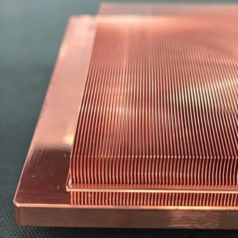
Diamond-Copper Thermally Conductive Composite. High thermal conductivity, tunable CTE, robust.
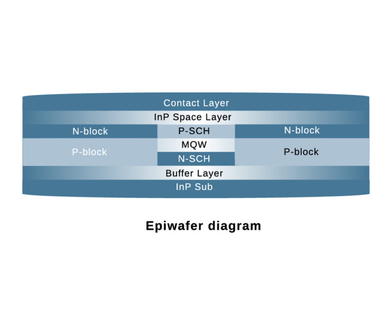
The DE-CW-1310 DFB EPI wafer, a high-performance epitaxial structure designed for distributed feedback (DFB) lasers operating at 1310 nm....
Ceramic thin-filmvacuum sensor Optical gas massflowmeter Liquid mass flowmeter Force sensor MEMS...
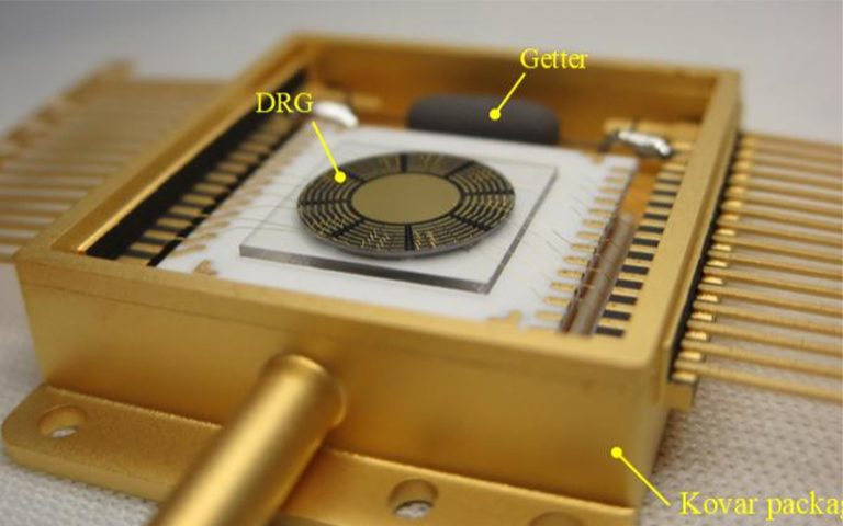
Photoelectric sensing chip Light source chips Optical transmission and modulationchips Optical detection and receptionchips...