
Selecting an optimal dfb laser chip for optical transceivers requires evaluating dynamic spectral purity, high-speed modulation response, and thermo-mechanical constraints. High-bandwidth telecommunication and data center interconnects rely on semiconductor laser diodes that maintain single-mode stability without excessive thermal degradation. Established in 2019, DEEPETCH specializes in high-density IC substrates, ceramic packages, and optical packaging components, serving over 1,560 clients globally across data center, AI computing, and cloud infrastructure networks. Evaluating optical transmitters involves analyzing chip architectures alongside packaging stack-ups to prevent signal distortion and thermal mismatch.
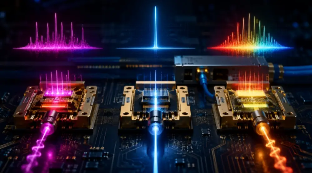
Evaluating laser diode behavior across high-speed optical links starts with examining internal cavity geometry and semiconductor material properties.
Fabry‑Perot (FP) lasers utilize cleaved semiconductor facets to form a reflective cavity, causing multi‑mode oscillation across broad spectral widths. In contrast, integrating a dfb laser chip built on Indium Phosphide (InP) substrates provides narrow single‑mode output. InP materials feature an electron mobility of 3,000–4,500 cm²/(V·s), supporting high‑frequency signal amplification and operational stability above 100 GHz. This spectral purity eliminates mode competition and lowers chromatic dispersion penalties in single‑mode fiber systems.
When evaluating a dfb laser vs eml laser setup, direct modulation speed limits and thermal dissipation become primary tradeoffs. Directly modulated DFB laser diodes vary drive current to generate optical pulses, achieving low power consumption of ≤ 10 W in 400G transceivers. However, Electro‑Absorption Modulated Lasers (EML) integrate an unmodulated laser section with an absorption modulator. While EMLs mitigate transient chirp over longer distances, directly modulated DFB chips reduce power consumption, circuit complexity, and assembly costs in short to medium‑reach applications.
Selecting the appropriate transmitter format requires weighing optical output power, side-mode suppression ratio, threshold current, and thermal drift against module assembly costs. For a comprehensive technical breakdown of single-mode laser diode architectures, review the guide on Detailed Introduction to Distributed Feedback (DFB) Laser Chips.
| Transmitter Parameter | Fabry-Perot (FP) Laser | Distributed Feedback (DFB) Chip | Electro-Absorption Modulated (EML) |
| Cavity Structure | Facet Reflector (Multi-Mode) | Internal Bragg Grating (Single-Mode) | DFB Source + EAM Modulator |
| Typical Reach | Multi-mode / Short Reach | Sub-500m to 10km Single-Mode | 2km to 10km+ Single-Mode |
| Transient Chirp | High | Moderate (Direct Modulation) | Low (External Modulation) |
| Power Consumption | Very Low | Low (≤ 10 W in 400G modules) | Moderate to High (≤ 16 W) |
Preserving signal integrity across multi-gigahertz channels demands tight control over spectral line broadening and unwanted longitudinal mode power.
Etching a diffraction Bragg grating directly into the active layer enforces longitudinal mode selection. InP-based direct bandgap energy (1.34 eV) aligns precisely with the 1310 nm and 1550 nm telecommunication windows. Integrating a dfb laser chip with built-in grating structures ensures that only the wavelength matching the Bragg condition passes through, locking the center wavelength under high-speed switching conditions.
Achieving a high side-mode suppression ratio exceeding 40 dB ensures that non-lasing secondary modes remain suppressed relative to the primary optical carrier. High suppression ratios prevent optical power distribution into secondary wavelengths, which otherwise triggers pulse spreading and chromatic dispersion degradation over long fiber spans.
High-speed laser drivers require low-loss interconnect routing between driver ICs, impedance matching networks, and laser dies. Deploying Custom IC Substrates (ABF Substrates) using Advanced Modified Semi-Additive Processes (amSAP) supports fine Line/Space specs down to 5/5 μm and 8/8 μm. These high-density ic packaging substrates lower parasitics and maintain signal fidelity across multi-channel transmitter sub-assemblies.
High drive currents and fluctuating ambient temperatures alter the effective refractive index of laser cavities, demanding effective thermal and packaging solutions.
Operating optical transceivers under standard conditions (3.3 V supply voltage and case temperatures from 0°C to 70°C) subjects laser chips to thermal expansion gradients . Maintaining the stability of a dfb laser chip requires controlling thermal drift, typically around 0.1 nm/°C. Without proper thermal paths, temperature spikes shift the Bragg reflection wavelength away from optical filter passbands, degrading link performance.
To insulate temperature-sensitive laser drivers and photodetectors from harsh operational environments, robust housing is essential. Integrating Ceramic Packaging Solutions (Pottery and Porcelain SOP) provides hermetic sealing with a helium leak rate under 1 × 10⁻⁸ atm·cc³/sec. Operating across temperatures from -55°C to +200°C with MSL3 preconditioning under JESD22‑A113I, these ceramic packages feature low thermal resistance (15–30°C/W), isolating sensitive optical components from moisture and mechanical stress.
Preventing reflection losses in high-frequency PAM4 drive circuits requires controlled impedance matching across the substrate interface. Implementing differential 100 Ω (± 10%) and single‑ended 50 Ω trace routing suppresses RF reflections. Controlling parasitic inductance along bond wires and micro-bumps minimizes high-speed distortion, assisting in effective dfb laser chirp control during rapid direct modulation.
Choosing the right optical transmitter format balances initial hardware expenditure, module manufacturing yield, and long-term operating power efficiency.
In intra-data center networks, deploying a directly modulated dfb laser chip in a 1310nm dfb laser module offers clear cost advantages over EML designs for distances up to 500 m. Single mode 400G DR4 optical transceivers operating with 1310 nm DFB lasers achieve data rates of 400Gbps PAM4 while keeping total module power consumption at or below 10 W, lowering power overhead across dense switch architectures.
Immersion liquid cooling has become a standard technique for Next-Generation-AI data centers due to the very high thermal dissipation. Liquid-cooled optical transceivers that have been designed using special packaging can operate very reliably within a case temperature range of 0°C up to 60°C. This allows for optical alignment as well as for stable output power when operating in a dielectric fluid.
Long-term laser reliability verification through rigorous screening prior to deployment is required. Burn-in testing, high-temperature storage tests (JESD22-A103), and temperature cycling (JESD22-A104) verify that the laser chip has stable threshold currents during its operational life-time and identifies early infant mortality failures.
Developing custom optical sub-assemblies and substrate stack-ups requires technical alignment from initial CAD thermal modeling through volume production.
DEEPETCH provides complete OEM, ODM, and JDM capabilities for high-speed optical modules and substrate packaging. Supported by experienced engineering teams, DEEPETCH delivers customized hardware solutions, from fine-pitch high-density ic packaging substrates to hermetic ceramic packages.
Engineers and procurement teams should evaluate key parameters before finalizing component orders:
By aligning thermal simulation, substrate stack-up design and packaging specifications early in the product development process, production can be ready on time and total unit cost can be lowered.
Addressing high-speed signal integrity, thermal dissipation, or custom packaging specifications for optical transmitters requires tailored engineering support. Optical engineers and procurement specialists seeking CAD layout reviews, substrate stack-up validation, or technical data sheets can submit project requirements through the DEEPETCH engineering contact channel to consult directly with technical teams.
A dfb laser chip incorporates a diffraction Bragg grating directly within the active semiconductor cavity. This grating enforces single-mode longitudinal emission with a narrow spectral linewidth, whereas a Fabry-Perot laser emits multiple longitudinal modes with broader spectral spreading, making it more susceptible to chromatic dispersion.
The Side-Mode Suppression Ratio (SMSR) is the optical power ratio of the main lasing mode to the highest secondary mode. By having an SMSR greater than 40 dB, the energy not in the desired wavelength is suppressed, which in turn reduces the chromatic dispersion penalty and allows for longer reach on single-mode fiber links.
Temperature fluctuations change the refractive index and physical dimensions of the active laser cavity, causing the Bragg emission wavelength to drift at approximately 0.1 nm/°C. Proper thermal management using high-conductivity ceramic packages or TEC cooling prevents wavelength drift away from multiplexer filter channels.

Molybdenum copper composite: adjustable CTE, high conductivity, lower density than tungsten copper. No...

Tungsten copper composite: low CTE, high conductivity. Ideal for RF, power, optical packaging.

Diamond-aluminum composite for advanced thermal management. Lightweight, high thermal conductivity, low...

Diamond-Copper Thermally Conductive Composite. High thermal conductivity, tunable CTE, robust.

The DE-CW-1310 DFB EPI wafer, a high-performance epitaxial structure designed for distributed feedback (DFB) lasers operating at 1310 nm....

Ceramic thin-filmvacuum sensor Optical gas massflowmeter Liquid mass flowmeter Force sensor MEMS...

Photoelectric sensing chip Light source chips Optical transmission and modulationchips Optical detection and receptionchips...

Using a“Detach Core”which has two-layers carrier foil structure on the surface as a core, and forming...

Tenting process is a kind of subtractive process, the process as follows: Laminating photosensitive film...

Modified Semi-Added Process abbreviated as mSAP, which can be used on the core or build-up layers, pattern...