
High-performance computing chips depend heavily on advanced multi-die integration to bypass physical lithography limits. Selecting the right CoWoS package substrate technology requires balancing thermal dissipation, interconnect density, and mechanical strain across heterogeneous dies. Established in 2019, DEEPETCH specializes in high-density substrates, wafer carriers, and advanced packaging solutions for data centers and AI compute nodes, having delivered tailored hardware architectures to over 1,560 global microelectronics clients. Managing thermal stress and yield loss across multi-chip modules requires strict substrate selection guidelines and process control benchmarks.
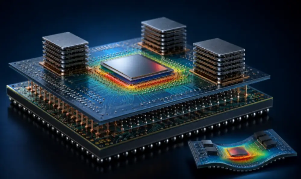
Integrating logic ICs and High Bandwidth Memory (HBM) on a single substrate introduces complex thermo-mechanical behaviors during reflow and operation.
Silicon interposers have a Coefficient of Thermal Expansion (CTE) of about 3.2 × 10⁻⁶/K. As a result of thermal expansion during 250°C reflow, significant thermal stress is incurred by the micro‑bumps on 25–55 µm pitch between adjacent silicon dies, and the organic package. This results in fatigue, localized delamination, and high joint shear strain in a CoWoS type package assembly.
Substrate thickness instability directly triggers planar warpage during processing. Maintaining a Total Thickness Variation (TTV) under 0.5 μm and a surface roughness Ra < 0.5 nm prevents Chemical‑Mechanical Planarization (CMP) edge chipping and vacuum seal leaks during carrier handling. Without stringent 2.5D interposer warpage limits, uneven stress distribution causes micro‑crack propagation across fine‑pitch redistribution layers.
Evaluating structural performance requires analyzing interconnect density against thermal impedance and mechanical stability. For detailed comparative engineering metrics across 2.5D integration formats, review the benchmark guide on How Does CoWoS Packaging Compare to Other 2.5D Packaging Technologies.
Selecting between full-surface interposers and localized bridge solutions impacts both thermal management strategies and front-end fabrication expenses.
Full-reticle silicon interposers (CoWoS-S) provide maximum interconnect density but face lithography mask limits exceeding 4,000 mm². In contrast, localized silicon bridges like CoWoS-L and EMIB embed small silicon dies into organic substrates. While bridges reduce raw material costs and bypass reticle constraints, managing silicon interposer thermal expansion across heterogeneous boundary interfaces remains a primary reliability concern.
Organic Redistribution Layer (RDL) substrates eliminate expensive silicon processing steps, offering lower insertion loss for high-speed signals. However, CoWoS-R and Fan-Out Chip-on-Substrate (FOCoS) structures exhibit higher CTE values than silicon, making them susceptible to substrate warpage under elevated operating temperatures.
Thinning $300\text{ mm}$ interposers down to sub-100 µm profiles requires rigid mechanical support during backside processing. Incorporating Glass Wafer carriers with optical transmittance exceeding 90% at 355 nm wavelength enables efficient ultra-thin wafer laser debonding. These ultra-flat borosilicate carriers maintain mechanical rigidity, preventing substrate bowing during high-temperature thermal release steps.
Routing high-frequency signals across multi-die modules demands precise trace geometries and robust environmental isolation for power delivery ICs.
Multi-channel HBM routing requires tight line-space controls to preserve signal integrity between memory stacks and logic processors. Implementing Custom IC Substrates (ABF Substrates) utilizing amSAP and SAP processes supports fine Line/Space features down to 5/5 μm and 8/8 μm. These high-density ABF IC substrates reduce transmission loss while supporting high-bandwidth signal fan-out.
Power management ICs and gate drivers placed adjacent to high-power compute nodes operate under extreme thermal conditions. Deploying Ceramic Packaging Solutions (Pottery and Porcelain SOP) guarantees reliable operation across temperatures ranging from -55°C to +200°C. Featuring MSL3 preconditioning under JESD22-A113I and certified under IATF 16949 and ISO 9001 standards, these ceramic packages prevent moisture ingress and mechanical fatigue in harsh operational environments.
Differential high-speed channels need to be controlled in impedance in order to avoid signal reflection and crosstalk. By maintaining a differential impedance of 100 Ω (± 10%) and single-ended impedance of 50 Ω, the eye patterns can be maintained for packages with multi-die CoWoS architectures. By shortening the micro-bump interconnects, parasitic inductance can be further reduced for high-speed channels with multi-gigahertz bandwidths.
Yield management in multi-die packaging directly governs commercial viability, requiring strict die qualification and substrate layer optimizations.
Assembling complex multi-die modules without prior chip screening risks compounding yield losses. Known Good Die (KGD) testing protocols ensure that only fully functional logic and memory dies enter the packaging line, minimizing total module scrap rates in complex CoWoS package manufacturing.
Balancing thermal dissipation and mechanical stress depends on FCBGA substrate stack-ups. Moving from 6+2+6 to 8+2+8 layer configurations provides additional power planes and thermal dissipation paths. The table below compares substrate stack-up metrics for high-density 2.5D assemblies:
| Substrate Stack-Up | Typical Thickness | Layer Count Balance | Thermal Dissipation Capability | Warpage Risk Level |
| 6+2+6 FCBGA | 1.2–1.4 mm | Moderate | Standard | Low to Moderate |
| 8+2+8 FCBGA | 1.6–1.8 mm | High | Enhanced Power/Ground Planes | Low (Symmetrical Design) |
Identifying micro-voids, delamination, and crack formation within micro-bump arrays requires high-resolution inspection. Non-destructive methods including Scanning Acoustic Microscopy (CSAM) and 3D X-ray tomography detect sub-micron voids in bonded interfaces, safeguarding long-term module reliability.
Translating 2.5D architecture designs into volume manufacturing requires dedicated technical collaboration from initial stack-up simulation to final testing.
DEEPETCH provides end-to-end OEM, ODM, and JDM engineering support, assisting clients with CAD layout reviews, thermal dissipation simulations, and custom substrate fabrication for advanced CoWoS package projects.
Engineering and procurement managers should verify the following parameters prior to finalizing packaging orders:
Evaluating custom substrate stack-ups, glass wafer carrier specifications, or ceramic packaging requirements requires early engineering alignment to optimize yield and thermal performance.
Addressing complex thermo-mechanical strain, CTE mismatch, or fine Line/Space substrate requirements requires precise design review and material alignment. Engineering teams seeking custom CAD evaluations, substrate stack-up validation, or technical data sheets can submit project specifications directly through the official DEEPETCH engineering contact channel to consult with packaging specialists.
The primary thermal limitation stems from the CTE mismatch between the silicon interposer (≈ 3.2 × 10⁻⁶/K) and the underlying organic substrate during 250°C reflow cycles. This mismatch induces thermal expansion gradients that generate shear strain on micro‑bump arrays, potentially causing delamination or joint fatigue.
Substrate Total Thickness Variation (TTV) exceeding 0.5 μm creates planar surface unevenness during Chemical‑Mechanical Planarization (CMP) and carrier bonding steps. This unevenness leads to vacuum leaks during handling, localized polishing defects, and micro‑bump bridging errors during die placement.
Ajinomoto Build‑up Film (ABF) substrates support fine line/space features down to 5/5 μm, providing high routing density for multi‑channel High Bandwidth Memory (HBM) connections while maintaining stable dielectric properties and controlled impedance across high‑frequency signal paths.

Molybdenum copper composite: adjustable CTE, high conductivity, lower density than tungsten copper. No...

Tungsten copper composite: low CTE, high conductivity. Ideal for RF, power, optical packaging.

Diamond-aluminum composite for advanced thermal management. Lightweight, high thermal conductivity, low...

Diamond-Copper Thermally Conductive Composite. High thermal conductivity, tunable CTE, robust.

The DE-CW-1310 DFB EPI wafer, a high-performance epitaxial structure designed for distributed feedback (DFB) lasers operating at 1310 nm....

Ceramic thin-filmvacuum sensor Optical gas massflowmeter Liquid mass flowmeter Force sensor MEMS...

Photoelectric sensing chip Light source chips Optical transmission and modulationchips Optical detection and receptionchips...

Using a“Detach Core”which has two-layers carrier foil structure on the surface as a core, and forming...

Tenting process is a kind of subtractive process, the process as follows: Laminating photosensitive film...

Modified Semi-Added Process abbreviated as mSAP, which can be used on the core or build-up layers, pattern...