
Silicon Carbide (SiC) and Gallium Nitride (GaN) power semiconductors allow converters to operate at higher switching frequencies and elevated voltages. However, because wide-bandgap dies are significantly smaller than equivalent silicon chips, heat generation is concentrated over a reduced surface area. Designing reliable SiC/GaN power systems requires managing extreme local heat dissipation to prevent thermal runaway and mechanical fatigue in die-attach layers.
Established in 2019, DEEPETCH provides microelectronics packaging, carrier substrates, and wafer processing support to over 1,560 global clients. The engineering group focuses on high-thermal-conductivity ceramic substrates, hermetic semiconductor packaging, and precision wafer carriers. By aligning substrate physical properties with power device thermal requirements, DEEPETCH delivers packaging architectures that maintain low thermal resistance across severe industrial and automotive operating cycles.
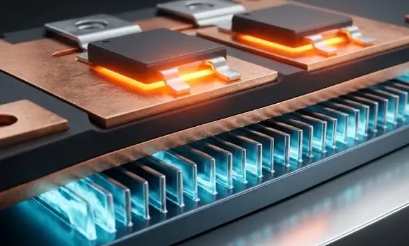
Migration from silicon to wide bandgap power devices changes the thermal profile of power modules. While the active junction limit increases, the high power density in power modules creates high temperature gradients within the internal package layers.
High-power SiC MOSFETs and GaN HEMTs operate at elevated junction temperatures between 300°C and 400°C. Because these wide-bandgap dies achieve low on-state resistance within small footprint areas, localized heat flux at active switching nodes exceeds conventional cooling capabilities. Without low-impedance dissipation paths, localized thermal hot spots form directly beneath the semiconductor junction, compromising gate oxide integrity and reducing overall conversion efficiency in high-density SiC/GaN power modules.
Solid-state power packages consist of stacked materials with varying thermal expansion behavior. When subjected to standard Thermal Cycling Tests (TCT) spanning -55°C to 125°C, coefficient of thermal expansion (CTE) mismatches generate shear stress at soldered interfaces. Repeated thermal expansion and contraction cause micro-cracking in die-attach layers, solder void growth, and wire bond lifting, ultimately raising the thermal resistance value between the chip junction and device outer shell.
System reliability depends on matching each material layer from the semiconductor die to the external liquid cold plate. For an engineering breakdown of heat flow paths and substrate selection criteria, review the reference technical guide on Thermal Management for Wide-Bandgap (SiC/GaN) Power Electronics.
Substrate layers form the core of the power module’s mechanical and thermal properties. Here, appropriate selection of ceramics and use of wafer handling carriers are crucial to distribute the heat generated within the module to the external heatsinks.
High-purity ceramic substrates are required for direct thermal dissipation and electrical isolation. Selecting between Aluminium Nitride (AlN) and Silicon Nitride (Si₃N₄) involves balancing ceramic substrate thermal conductivity against mechanical toughness.
| Ceramic Material | Thermal Conductivity (W/m⋅K) | Flexural Strength (MPa) | Primary Packaging Application |
|---|---|---|---|
| Aluminium Nitride (AlN) | 170 – 230 | 300 – 400 | Maximum heat dissipation in continuous high-power modules |
| Silicon Nitride (Si₃N₄) | 60 – 90 | 600 – 800 | High thermomechanical stress & automotive power cycling |
| Alumina (Al₂O₃) | 20 – 30 | 350 – 400 | Standard power density & cost-sensitive industrial drives |
In high-power switching applications, maintaining stable junction temperatures in SiC/GaN power circuits requires choosing substrates that balance peak thermal conductivity with flexural strength under cyclic mechanical loads.
Before active dies are bonded to high-conductivity ceramic substrates, raw SiC and GaN wafers undergo extreme back-grinding down to sub-100 μm thicknesses to lower vertical resistance. To prevent lattice fracture during this pre-assembly phase, integrating Glass Wafer Carrier Solutions provides the temporary rigid support and planar stability required prior to substrate metallization. These glass carriers feature optical transmittance exceeding 90%, surface roughness under 0.5 nm, and electrical resistivity greater than 10^16 Ω·cm.
The interfacial layer or layers account for a significant portion of the total die-attach thermal impedance. By replacing conventional lead-free solders with a transient liquid phase bonding (TLPB) material or a sintered silver paste, the low conductivity intermetallic phases, typically found in soldered interfacial layers, are eliminated. Sintered silver paste, for example, offers thermal conductivity values greater than 150 W/m·K, resulting in low thermal impedance values even under elevated continuous operating temperatures.
For operation at high frequencies, power devices from SiC and GaN need appropriate packaging, in order to keep parasitic inductance as low as possible and to withstand ambient temperatures.
For power devices deployed in aerospace or automotive environments, DEEPETCH manufacturesCeramic Packaging Solutions (Ceramic SOP). Designed for operating temperature ranges from -55°C to +200°C, these hermetic packages pass MSL3 preconditioning tests under JESD22-A113I. Fabricated under certified IATF 16949 and ISO 9001 quality systems, ceramic SOP housings shield active power dies from moisture ingress while conducting heat away from gate structures.
High-speed gate drivers controlling wide-bandgap switches require tight trace routing to prevent voltage overshoot. Utilizing Custom IC Substrates based on Ajinomoto Build-up Film (ABF), DEEPETCH incorporates laser mask projection dimple designs for enhanced silver adhesion and inside-substrate chip setups. These high-density interconnect substrates comply with SFF-8431 and SFF-8432 standards, reducing parasitic inductance in gate drive circuits.
To ensure long-term survival of modules in the field, the encapsulated power assemblies are subject to strict inspection using non-destructive analytical test methods. These test methods – including 3D X-ray inspection as well as SEM, TEM, TDR and FIB sectioning – detect for example internal solder voids, delamination seams as well as wire bond damage prior to dispatch of the respective solar module.
When conductive substrate layers alone cannot keep junction temperatures below maximum thresholds, active and interface cooling methods must be integrated into the module assembly.
Small surface roughness on the ceramic substrate baseplate and liquid cold plate creates high thermal contact resistance by trapping air in microscopic contact areas. By applying phase-change thermal interface materials (TIMs) or liquid metal eutectic alloys, the air is displaced and, under pressurization, the materials conform to the mating surface, reducing interface thermal resistance to a fraction of that of typical silicone greases.
For extreme power density applications, microchannel liquid cooling cold plates route fluid directly beneath the ceramic substrate. Utilizing liquid-cooled cold plates and immersion cooling transceivers supporting high power dissipation up to 14W per node, modern cooling architectures for industrial SiC/GaN power conversion eliminate baseplate layers entirely, dropping overall thermal resistance from junction to coolant.
Moisture accumulation within package voids causes localized pressure buildup during high-temperature operation. Modules undergo Bi-Directional Highly Accelerated Stress Testing (BHAST) at 130°C and 85% relative humidity for 168 hours to verify that die-attach interfaces and encapsulation materials resist delamination under combined moisture and bias conditions.
Implementing customized substrate architectures and packaging lines requires coordinating material selection with manufacturing capabilities.
Supporting commercial SiC/GaN power projects, DEEPETCH operates certified cleanroom facilities and precision packaging lines. Servicing over 1,560 global clients since its establishment in 2019, the company provides turnkey OEM/ODM engineering—from initial thermal simulation and substrate metallization to final hermetic sealing and electrical testing.
Before issuing manufacturing specifications for custom power packaging, evaluate the following parameters:
Engineers managing thermal design challenges or evaluating packaging options for custom SiC/GaN power packages can submit 2D/3D CAD files and thermal boundaries to the DEEPETCH technical team for contact. The engineering staff assists with substrate selection, material compatibility checks, and prototype packaging specifications.
Q1: How does localized heat flux affect SiC/GaN power efficiency?
A: Because SiC and GaN dies are smaller than silicon devices of equivalent power ratings, heat generation is concentrated over a smaller area. Unmanaged heat flux increases junction temperatures, raising on-state resistance (RDS(on)) and driving conduction losses higher, which degrades overall system conversion efficiency.
Q2: What is the benefit of using an AlN substrate over an Al₂O₃ substrate?
A: Using Aluminium Nitride (AlN) ceramic substrate material provides high thermal conductivity of 170 to 230 W/m·K compared to Alumina (Al₂O₃) at 20 to 30 W/m·K. This high thermal conductivity allows for low junction-to-case thermal resistance in high power density switching applications.
Q3: Why is hermetic ceramic sop packaging required for high-temperature power electronics?
A: Hermetic ceramic packaging is used for Hermetic packaging of active power dies. This packaging type is highly resistant to moisture, chemicals and thermal oxidation. It remains mechanically sound over a temperature range of -55°C up to +200°C. The hermetic ceramic packaging does not delaminate in very harsh industrial and automotive environment.

Molybdenum copper composite: adjustable CTE, high conductivity, lower density than tungsten copper. No...

Tungsten copper composite: low CTE, high conductivity. Ideal for RF, power, optical packaging.

Diamond-aluminum composite for advanced thermal management. Lightweight, high thermal conductivity, low...

Diamond-Copper Thermally Conductive Composite. High thermal conductivity, tunable CTE, robust.

The DE-CW-1310 DFB EPI wafer, a high-performance epitaxial structure designed for distributed feedback (DFB) lasers operating at 1310 nm....

Ceramic thin-filmvacuum sensor Optical gas massflowmeter Liquid mass flowmeter Force sensor MEMS...

Photoelectric sensing chip Light source chips Optical transmission and modulationchips Optical detection and receptionchips...

Using a“Detach Core”which has two-layers carrier foil structure on the surface as a core, and forming...

Tenting process is a kind of subtractive process, the process as follows: Laminating photosensitive film...

Modified Semi-Added Process abbreviated as mSAP, which can be used on the core or build-up layers, pattern...