
For semiconductor thin films, spin coating usually offers better thickness uniformity and repeatability, while drop casting is often more practical for thick films, scarce precursor solutions, or early-stage laboratory work. The right choice depends on target thickness, solution viscosity, substrate wettability, solvent evaporation, equipment capability, and the quality requirements of the finished device.
The broad phrase “drop casting vs. spin coating” is used by both materials researchers and semiconductor engineers. This guide keeps the comparison focused on wafer coating, photoresist and passivation work, thin-film characterization, and thick functional layers. DEEPETCH supplies glass, compound-semiconductor, and ceramic substrates that can be specified for coating and post-deposition processes.
Precision is not one number. A qualified coating process must control thickness, across-substrate uniformity, surface roughness, defect density, repeatability, and compatibility with later lithography, etch, cure, or electrical steps.
Local thickness variation can change resistance, capacitance, optical absorption, dielectric strength, or etch depth. Surface roughness and substrate topography also affect wetting, focal depth, line-edge definition, and the stability of a later layer. A useful specification should state the measurement method, sampling points, edge-exclusion rule, and temperature or humidity conditions.
Contact angle and surface energy influence whether a liquid spreads or retracts. During drying, solvent volatility, ambient airflow, humidity, and temperature can create pinholes, striations, coffee-ring deposits, voids, or edge beads. These variables matter to both methods, but drop casting is generally more exposed to passive evaporation gradients because the substrate is stationary.
Evaluating process metrics requires systematic comparisons of film thickness tolerances, deposition velocity, and precursor consumption. Process engineers frequently reference established engineering data when determining method capability boundaries. For detailed technical benchmarking metrics regarding these two deposition methods, review the drop casting vs spin coating comparison guide.
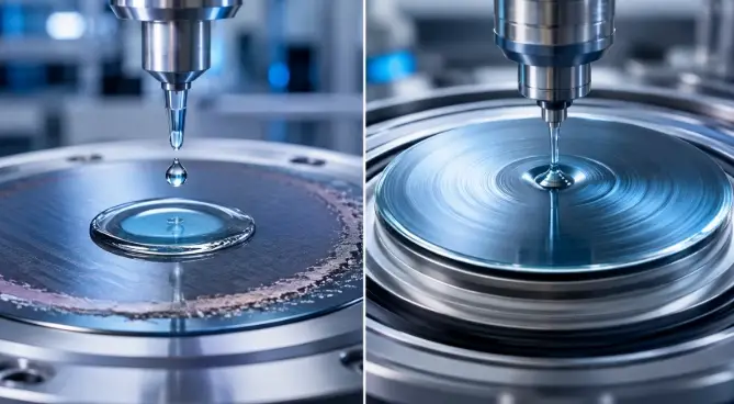
The physical difference is simple: spin coating uses controlled rotation to spread a liquid, while drop casting relies on dispensed volume, wetting, gravity, and solvent evaporation on a stationary substrate. Their process windows are therefore different.
Spin coating is controlled through variables such as dispense volume, solution viscosity, acceleration, rotation speed, spin time, solvent volatility, and ambient conditions. Rotation drives excess liquid toward the edge while viscous and evaporative effects set the final film. It is commonly selected for thin, uniform layers where repeatability and lithography compatibility matter.
The process still needs edge-bead management, exhaust control, bowl cleanliness, and a calibrated recipe. A higher rotation speed does not automatically produce a better film; the result depends on the fluid and substrate.
Drop casting places a measured liquid volume on a stationary substrate and allows it to spread and dry. It can retain most of the dispensed material and can handle concentrated solutions, slurries, and thicker functional layers that are difficult to distribute by rotation. The drawbacks are slower drying, greater sensitivity to wetting and evaporation gradients, and weaker control of cross-substrate uniformity unless the process is carefully engineered.
| Decision factor | Spin coating | Drop casting |
| Thin-film precision | Strong when the fluid and recipe are qualified | Usually limited by wetting and evaporation gradients |
| Repeatability | High potential with calibrated equipment and stable materials | More sensitive to dispensing and drying conditions |
| Thickness range | Best suited to thin and moderately thick layers | Useful for thick films and concentrated formulations |
| Material utilization | Lower because excess liquid is expelled | Higher because the dispensed volume remains on the substrate |
| Substrate shape | Most convenient on rigid, balanced wafers or panels | More tolerant of irregular or non-rotating substrates |
| Scale-up | Well suited to automated wafer lines | Better for laboratory work or selected thick-film processes |
| Main risks | Edge bead, particle contamination, recipe drift | Coffee-ring effect, long drying time, non-uniform edges |
| Typical use cases | Photoresist, passivation, planar thin films, optical coatings | Thick functional layers, screening formulations, early R&D |
| Cost question | Requires a coater, bowl, exhaust, and recipe control | Lower equipment complexity but longer cycle time may limit throughput |
For semiconductor production, spin coating is normally the starting point when the layer must be thin, uniform, repeatable, and compatible with automated lithography. Drop casting can be the better option when material conservation, high viscosity, thick-film deposition, or laboratory flexibility matters more than wafer-scale uniformity.
Photoresist, dielectric, and passivation processes usually require controlled thickness and a clean, repeatable edge profile. Spin coating provides a recipe-based path, but the substrate must have suitable flatness, surface energy, and cleanliness. A coating trial should record dispense volume, acceleration, rotation profile, drying conditions, and measurement results.
Drop casting is useful for screening a new precursor or conserving a limited formulation. It can reveal whether a material forms a film before an automated tool is commissioned. Once the project moves toward volume production, engineers should test whether spin coating, slot-die coating, spray coating, or another scalable method can meet the required uniformity and cycle time.

Choose spin coating when most of the following are true: the target layer is thin, the substrate is rigid and balanced, uniformity and repeatability are key, the solution viscosity is suitable for rotation, and a controlled coating tool is available.
Choose drop casting when most of the following are true: the layer is thick, the precursor is expensive or limited, the solution is highly viscous or contains particles, the substrate is irregular, or the work is still at laboratory scale.
In either case, qualify substrate wettability, solvent system, ambient conditions, drying profile, inspection method, and defect limits before comparing suppliers or releasing a production recipe.
Substrate flatness, roughness, crystal orientation, thermal stability, and chemical compatibility directly affect liquid flow and film defects.
An ultra-flat Glass Wafer can provide a stable reference surface for spin coating, photolithography, and optical characterization. Confirm the wafer diameter, thickness, TTV, roughness, surface treatment, cleaning chemistry, and optical requirement with the coating tool. A flat wafer helps, but it cannot compensate for poor wetting or an unstable recipe.
Gallium Arsenide (GaAs) substrates are used in high-frequency and optoelectronic device work where the crystal orientation, surface preparation, and thermal budget matter. Before coating, define the surface condition, resist or passivation chemistry, bake profile, and edge-bead strategy. The coating method should be selected with the device process—not the substrate name alone—in mind.
An Alumina Ceramic Substrate can support thick-film work that includes solvent removal, curing, or sintering. Its value comes from mechanical rigidity, chemical resistance, and thermal stability, but the grade, geometry, surface finish, and thermal cycle still need to be specified.
DEEPETCH can review custom dimensions, dicing, double-side polishing, edge profiling, surface functionalization, and material selection for glass, ceramic, and compound-semiconductor substrates. A useful request should include the coating method, solution or film type, target thickness, wettability requirement, thermal cycle, cleaning chemistry, equipment interface, inspection method, and quantity.
For film-uniformity problems or a new substrate qualification, submit drawings and process requirements through the contact page for technical evaluation and sample planning.
Spin coating generally provides better thin-film uniformity and repeatability when the solution, substrate, equipment, and recipe are qualified. Drop casting is more suitable for thick layers or material-limited experiments where near-total retention is more valuable than wafer-scale uniformity.
Use drop casting when the precursor is expensive or scarce, the formulation is highly viscous or particle-loaded, the target layer is thick, the substrate is irregular, or the work is still at laboratory scale. Confirm drying time, edge variation, and defect acceptance before using it for a device process.
Poor or non-uniform wettability can cause de-wetting, striations, voids, and local thickness changes during rotation. Measure or control surface preparation, contact angle, cleanliness, and coating chemistry before changing the rotation recipe.
Provide substrate material, diameter, thickness, TTV, roughness, crystal orientation where relevant, surface treatment, coating chemistry, target thickness, thermal and cleaning conditions, edge requirements, inspection method, and required quantity.

Molybdenum copper composite: adjustable CTE, high conductivity, lower density than tungsten copper. No...

Tungsten copper composite: low CTE, high conductivity. Ideal for RF, power, optical packaging.

Diamond-aluminum composite for advanced thermal management. Lightweight, high thermal conductivity, low...

Diamond-Copper Thermally Conductive Composite. High thermal conductivity, tunable CTE, robust.

The DE-CW-1310 DFB EPI wafer, a high-performance epitaxial structure designed for distributed feedback (DFB) lasers operating at 1310 nm....

Ceramic thin-filmvacuum sensor Optical gas massflowmeter Liquid mass flowmeter Force sensor MEMS...

Photoelectric sensing chip Light source chips Optical transmission and modulationchips Optical detection and receptionchips...

Using a“Detach Core”which has two-layers carrier foil structure on the surface as a core, and forming...

Tenting process is a kind of subtractive process, the process as follows: Laminating photosensitive film...

Modified Semi-Added Process abbreviated as mSAP, which can be used on the core or build-up layers, pattern...