
CoWoS packaging improves high-performance semiconductor assembly by placing logic dies and high-bandwidth memory (HBM) close together on an interposer before the module is attached to a package substrate. The shorter electrical paths support higher interconnect density, lower signal delay, and more efficient heterogeneous integration than a conventional board-level approach. The trade-off is greater sensitivity to warpage, thermal expansion mismatch, temporary bonding, and carrier quality.
As AI accelerators and high-performance computing devices continue to combine large logic dies with multiple HBM stacks, these process controls have become as important as the package architecture itself. This guide explains the CoWoS structure, the main CoWoS variants, the bottlenecks that affect yield, and how engineers can select carrier materials for advanced packaging work. DEEPETCH supplies glass wafers, ceramic substrates, and custom substrate processing for semiconductor and microelectronics applications.
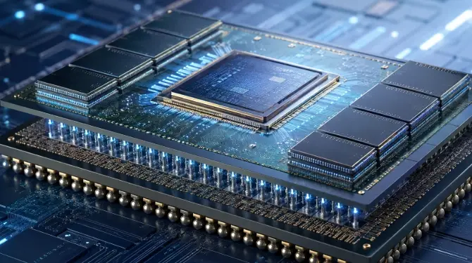
CoWoS means Chip-on-Wafer-on-Substrate. The name describes a two-stage assembly path: dies are integrated on an interposer, and the combined structure is then mounted on a package substrate. The interposer provides fine-pitch routing between chiplets, processors, and memory stacks while the package substrate connects the module to the system board.
In a typical 2.5D arrangement, GPU or ASIC dies sit beside HBM stacks rather than being connected through long board traces. The interposer contains dense redistribution structures and, in silicon-based designs, through-silicon vias (TSVs). This arrangement reduces the distance between computation and memory, which helps control latency and I/O power while allowing different process nodes or functions to be integrated in one package.
The benefit is architectural, not just dimensional: the package can combine logic, memory, and other chiplets without forcing every function onto one monolithic die. The final result still depends on signal integrity, thermal design, assembly tolerances, and package reliability.
CoWoS is useful when a product needs more bandwidth, more I/O, or heterogeneous integration than a standard organic package can provide. It does not automatically solve heat removal, cost, or manufacturing complexity. Large packages require a coordinated design for interposer routing, HBM placement, power delivery, thermal spreading, underfill, and final test.
For a technical overview of the architecture and material decisions, see the CoWoS packaging reference guide. Use it as background, then validate every design rule against the selected foundry, OSAT, and equipment process window.
The CoWoS family is not a single interposer construction. The right variant depends on package size, routing density, memory configuration, thermal budget, and manufacturing constraints.
| Variant | Interposer approach | Typical reason to consider it | Main engineering question |
| CoWoS-S | Silicon interposer with TSV-based vertical connections | Very dense routing for high-performance logic and HBM | Can the interposer size, thermal path, and assembly yield meet the package target? |
| CoWoS-R | RDL-based interposer using polymer and copper routing | Flexible chiplet and memory integration without a full silicon interposer | Are RDL warpage, line/space, and thermal limits suitable for the design? |
| CoWoS-L | RDL combined with local silicon interconnect structures | Larger integration areas and complex heterogeneous packages | How will local interconnect placement, reticle limits, and thermal stress be controlled? |
These labels should not be treated as interchangeable marketing terms. A design review should record the selected variant, interposer material, RDL or TSV structure, package dimensions, HBM configuration, and assembly flow.
The interposer is only one part of the yield equation. Carrier flatness, edge geometry, bonding chemistry, thermal cycling, and inspection method can all create defects before final test.
Silicon, organic substrates, metals, mold compounds, and adhesives expand at different rates. During bonding, reflow, cure, and cooling, that mismatch can bend the package or add shear stress at die and interposer interfaces. Excessive warpage may reduce micro-bump alignment margin, increase open or bridged joints, and complicate downstream handling.
Engineers should define the coefficient of thermal expansion (CTE) of each stack member over the actual process temperature range. A single room-temperature CTE value is not enough for a qualification plan.
Interposer thinning and TSV exposure often require a rigid carrier. Total thickness variation (TTV), surface roughness, bow, and edge profile affect grinding, chemical-mechanical planarization, vacuum sealing, and debonding. A carrier specification should therefore be tied to the tool chuck, adhesive, wafer diameter, loading method, and inspection equipment instead of copied from a generic datasheet.
For a 300 mm process, the control plan should define how TTV and bow are measured, where edge exclusion begins, and how rejected carriers are segregated. This makes the specification auditable and prevents a nominal flatness value from being mistaken for a guaranteed process yield.
CoWoS assemblies experience thermal exposure during cure, reflow, burn-in, and reliability testing. Carrier plates and fixtures must retain their geometry, resist chemical attack, and avoid particles or outgassing that could contaminate the package. Thermal spreading is also a system issue: a fixture can support a process, but it cannot replace package-level heat-spreader and cooling design.
Material selection should start with the process step, then move to the required geometry and inspection method.
An ultra-flat glass wafer can provide a stable reference surface for temporary bonding and thinning. Optical transmission may also be required when a UV laser debonding step is used. Before ordering, confirm wafer diameter, thickness, TTV, roughness, bow, edge bevel, chemical compatibility, and the laser wavelength used by the tool.
Alumina ceramic is suited to rigid fixtures and carrier plates that face repeated heating, cleaning, or burn-in. Its usefulness depends on the grade, geometry, surface finish, thermal profile, and handling system. Ask for a drawing-based review when the fixture must control flatness, avoid particle generation, or fit an automated loader. The Alumina Ceramic Substrate page provides the relevant product route.
Before releasing a carrier or fixture purchase, document:
Custom carrier work often requires more than a material name. DEEPETCH can review drawings and process conditions for dicing, lapping, polishing, edge profiling, coating, and substrate geometry across glass, ceramic, and semiconductor materials. The engineering discussion should include the tool interface, thermal cycle, optical requirement, surface specification, and expected inspection method.
If you are troubleshooting warpage, temporary-bond failure, carrier handling, or fixture life, send the relevant drawings and process conditions through the contact page for technical evaluation and sample planning.
A glass carrier supports wafer thinning, grinding, planarization, and TSV exposure while maintaining a controlled reference surface. If laser debonding is used, its optical properties must also match the laser process. Diameter, TTV, bow, roughness, adhesive, and debonding conditions should be specified together.
There is no universal answer. CoWoS-S, CoWoS-R, and CoWoS-L address different interposer, routing, package-size, and thermal constraints. The selection should be made from the accelerator die size, HBM arrangement, routing density, thermal design, and qualified assembly flow.
Different expansion rates create stress during heating and cooling. That stress can contribute to warpage, micro-bump alignment loss, cracking, or delamination. The correct check is a temperature-dependent stack analysis tied to the actual bonding, reflow, cure, and reliability profile.
Provide the wafer diameter, thickness, TTV, bow, roughness, edge profile, bonding material, thermal cycle, chemical exposure, optical requirement, tool interface, inspection method, and target quantity. Drawings and sample parts make a technical review more reliable.

Molybdenum copper composite: adjustable CTE, high conductivity, lower density than tungsten copper. No...

Tungsten copper composite: low CTE, high conductivity. Ideal for RF, power, optical packaging.

Diamond-aluminum composite for advanced thermal management. Lightweight, high thermal conductivity, low...

Diamond-Copper Thermally Conductive Composite. High thermal conductivity, tunable CTE, robust.

The DE-CW-1310 DFB EPI wafer, a high-performance epitaxial structure designed for distributed feedback (DFB) lasers operating at 1310 nm....

Ceramic thin-filmvacuum sensor Optical gas massflowmeter Liquid mass flowmeter Force sensor MEMS...

Photoelectric sensing chip Light source chips Optical transmission and modulationchips Optical detection and receptionchips...

Using a“Detach Core”which has two-layers carrier foil structure on the surface as a core, and forming...

Tenting process is a kind of subtractive process, the process as follows: Laminating photosensitive film...

Modified Semi-Added Process abbreviated as mSAP, which can be used on the core or build-up layers, pattern...