
Custom wafer carrier trays for compound semiconductor wafers must be designed around the wafer, not selected from a generic catalog. For GaAs, GaN, SiC, InP, and other non-standard substrates, the key decisions are tray material, ESD behavior, pocket geometry, dimensional tolerance, cleanroom compatibility, and downstream automation. A procurement-ready design should also define supported wafer sizes, CAD requirements, prototype flow, and the conditions that determine MOQ and lead time.
Established in 2019, DEEPETCH provides semiconductor materials, packaging, substrate, and engineering support for global customers. For custom wafer handling projects, the practical value is not only producing a tray shape, but matching carrier geometry to wafer thickness, bow, edge condition, process temperature, ESD targets, and automated handling requirements. This engineering-first approach helps reduce edge damage, contamination, and positioning errors before fragile compound semiconductor wafers move into dicing, bonding, or final packaging.
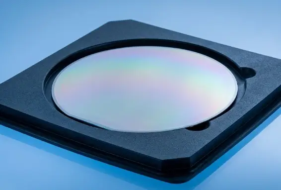
Generic silicon shipping trays are often built around standardized thickness, flatness, and handling assumptions. Compound semiconductor wafers can depart from those assumptions because they may be more brittle, more expensive per wafer, thinner after grinding, or processed with chemistries and temperatures that demand different carrier materials. The tray therefore becomes part of the process-control system rather than simple packaging.
GaAs is a high-electron-mobility III-V material, with electron mobility commonly around 8,500 cm²/(V·s), but its crystal structure is also vulnerable to edge chipping and cleavage damage. Other compound substrates such as GaN, SiC, and InP present different combinations of hardness, brittleness, epitaxial sensitivity, and surface requirements. A custom compound semiconductor wafer tray should therefore control shock, edge contact, static charge, and pocket clearance without touching active or polished center areas.
For inter-facility transport, vibration-damping features and controlled lid clearance help prevent wafer movement. For in-process handling, pocket support must keep the wafer stable enough for operators, vacuum wands, or robotic end effectors to pick it repeatedly without scraping the bevel or backside.
Compound semiconductor wafers are frequently thinned, bonded, epitaxially grown, or metallized before final singulation. That creates non-standard thickness, bow, and backside conditions that stock trays may not accommodate. A pocket that is too shallow can clamp a bowed wafer; a pocket that is too deep can allow vertical rattle. Both conditions increase the risk of micro-cracks, edge damage, or robotic pickup errors.
Balancing wafer bow, total thickness variation (TTV), lid clearance, and edge support requires a precision-fit carrier. For a deeper breakdown of structural carrier configurations and pocket layouts, review the reference technical guide on How to Custom Wafer Carrier Trays for Compound Semiconductor Wafers.
The tray specification should identify the wafer material because each substrate creates a different handling priority. The table below is a practical starting point for engineering review rather than a fixed catalog limitation.
| Wafer Type | Typical Handling Concern | Tray Design Focus | Common Custom Inputs |
| GaAs | Brittle cleavage, edge chipping, ESD-sensitive processing | Edge-contact support, vibration control, static-dissipative material | Diameter, thickness, bevel, bow, ESD target |
| GaN | Epitaxial surface protection, thin-wafer or bonded-wafer handling | Center-area clearance, flat support, contamination control | Substrate stack, active-side orientation, temperature, cleanroom class |
| SiC | Hard substrate with costly polished surfaces and tight automation needs | Accurate pocket geometry, abrasion-resistant clean material, repeatable pickup position | Diameter, thickness, backside condition, automation interface |
| InP | Fragile III-V substrate and sensitive edge condition | Low-contact pocket geometry, shock control, controlled retention | Diameter, thickness, edge profile, shipping or process use |
Material selection should be driven by the actual process environment. A polymer can be dimensionally stable yet unsuitable for wet chemistry, or chemically resistant yet too soft for precision automation. For custom wafer carrier trays, the main selection factors are surface resistivity, working temperature, chemical exposure, outgassing, particle generation, rigidity, and cleanroom compatibility.
Electrostatic discharge can damage sensitive epitaxial structures or active device features. An ESD-safe custom wafer carrier therefore needs a controlled static-dissipative range rather than simply being labeled “conductive.” For projects requiring ESD control, a target surface resistivity range such as 10⁴–10⁹ Ω/sq should be confirmed during material qualification and verified on finished carriers.
| Polymer Material | Continuous Working Temperature | Chemical Resistance | Primary Processing Application |
| PEEK (Carbon-Filled) | Up to 260°C | Excellent (Acids, Solvents) | High-temperature baking and precision carrier trays |
| PFA / PTFE | Up to 200°C | Superior (Etch Acids) | Wet chemical processing and cleaning cassettes |
| Conductive PP | Up to 90°C | Moderate | Room-temperature shipping and storage trays |
For high-temperature processing or bake-out steps, carbon-filled PEEK can provide better dimensional stability than lower-temperature commodity polymers. This matters when pocket depth, edge support, and robotic pickup coordinates must remain consistent after repeated thermal exposure. For room-temperature storage and shipping, conductive polypropylene can be a more economical choice when high-temperature resistance and aggressive chemical compatibility are not required.
In ISO Class 4 and Class 5 environments, the tray itself can become a contamination source. Low-grade conductive plastics may shed particles or introduce volatile residues. Material qualification should therefore consider particle generation, outgassing, ionic contamination, and resistance to the customer’s cleaning chemistry. Where required, ultrasonic cleaning and cleanroom packing should be defined as part of the manufacturing flow rather than treated as an afterthought.
When compound wafers are thinned to the point that self-supporting handling becomes unreliable, temporary carrier substrates are used to maintain flatness during back-grinding, metallization, inspection, and debonding. This is a different function from a shipping tray, but it is part of the same wafer-handling strategy.
For wafer thinning, back-grinding, and backside processing, Glass Wafer Carrier Solutions can be used as rigid temporary support during bonding and debonding steps. Optical transmission and surface flatness are important when the process relies on optical alignment or laser debonding through the carrier.
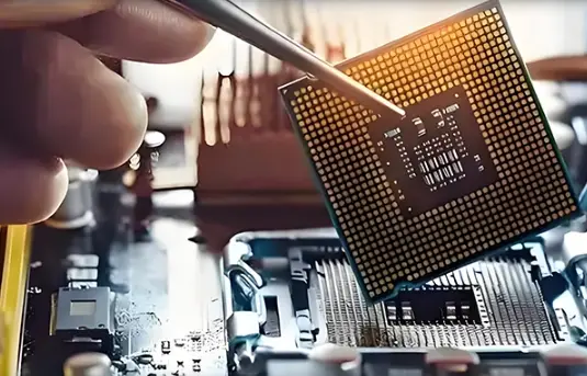
Glass carriers also provide strong electrical isolation for characterization and selected high-frequency test configurations. This helps reduce leakage paths and unwanted parasitic coupling when the carrier is used as a temporary support or isolation layer during measurement.
For a reusable wafer tray, pocket architecture should keep contact away from active center areas. Edge-contact designs support the wafer at the bevel or controlled perimeter zones. Retaining rings, lid inserts, or other hold-down features can be designed around the measured wafer bow so the substrate remains stable without excessive center pressure. The final geometry should be checked against wafer warpage, TTV, and the pickup method used on the customer’s line.
A custom wafer carrier does not operate in isolation. After dicing, the same dimensional discipline affects die transfer, singulation, bonding, and package assembly. Tray pocket position and repeatability therefore need to match the equipment that receives the wafer or die next.
Once compound semiconductor wafers are diced, individual dies may move into high-reliability packages. For applications that require hermetic sealing and wide operating temperature capability, DEEPETCH provides Ceramic Packaging Solutions (Ceramic SOP). The packaging stage should be considered during carrier design because die orientation, pickup position, and downstream bonding equipment can influence tray pocket layout.
For high-frequency digital and mixed-signal devices cut from compound wafers, singulated dies may be transferred into advanced substrate bonding processes. DEEPETCH also provides Custom IC Substrates based on ABF build-up structures for high-density routing. Linking carrier design with the later substrate and package flow helps engineering teams avoid orientation conflicts and unnecessary re-handling.
Automated pick-and-place equipment requires predictable wafer or die positioning. If pocket position or clearance is too loose, parts can shift during transit and move outside the robot’s expected pickup window. For precision automated handling, pocket tolerances are commonly reviewed in the ±0.02 mm to ±0.05 mm range when the design and manufacturing method support it. The correct tolerance should be set from the actual wafer dimensions, tray material, molding or machining process, and robot end-effector geometry rather than copied from a generic specification.
A sourcing decision should make it easy to answer one question: can the supplier turn your wafer and process data into a repeatable carrier specification? The following capability matrix converts that question into concrete RFQ items.
| Specification Item | Custom Capability / Engineering Input | What the Buyer Should Provide |
| Wafer Material | GaAs, GaN, SiC, InP, silicon and other project-specific substrates | Material / epitaxial stack / active-side orientation |
| Wafer Diameter | Standard and non-standard diameters reviewed by drawing | Nominal diameter and tolerance |
| Wafer Thickness | Standard, thinned, bonded, or non-standard thickness | Nominal thickness, TTV, maximum bow / warp |
| Pocket Geometry | Edge-contact, perimeter support, lid retention, custom depth / clearance | Bevel profile, backside condition, no-contact zones |
| Tray Material | Carbon-filled PEEK, PFA/PTFE, conductive PP, or project-qualified alternatives | Temperature, chemicals, vacuum / outgassing constraints |
| ESD Control | Static-dissipative material target can be specified by project | Required surface resistivity / ESD class |
| Dimensional Tolerance | Defined according to machining or molding method and automation needs | Robot pickup window, datum scheme, critical dimensions |
| Cleanroom / Cleaning | Ultrasonic cleaning and cleanroom handling can be included when required | Cleanroom class, cleaning chemistry, packing requirement |
| CAD Support | 2D drawing and 3D model review | STEP / STP / DXF / PDF or equivalent drawings |
| Prototype / Sampling | Prototype path confirmed after design and material review | Sample quantity and validation criteria |
| MOQ | Project-dependent; confirmed after material, tooling, and process review | Expected annual or batch volume |
| Lead Time | Project-dependent; prototype and production timing confirmed after CAD review | Required delivery date and approval schedule |
DEEPETCH executes a structured five-step engineering workflow for custom carriers:
Before finalizing a custom carrier order, engineering and procurement teams should confirm:
Engineers preparing new GaAs, GaN, SiC, InP, or other substrate runs can submit 2D/3D CAD models and process specifications directly to the DEEPETCH engineering team for contact. The technical team can review pocket geometry, polymer suitability, ESD requirements, cleanroom handling, and automation interfaces before sampling.
MOQ and lead time are not treated as one fixed number because they depend on tray material, machining or mold tooling, pocket count, cleaning requirements, prototype quantity, and expected production volume. After CAD review, the project can be divided into prototype validation and production release so buyers receive a clear sampling plan, acceptance criteria, and delivery schedule instead of a generic catalog commitment.
For the fastest RFQ review, submit the wafer drawing, maximum bow, process temperature, chemical exposure, ESD target, required cleanroom class, automation method, sample quantity, expected annual volume, and target delivery date. This allows the tray design to be quoted as a technical solution rather than only as a plastic part.
Standard trays are typically designed around common silicon wafer dimensions and handling assumptions. GaAs, GaN, and other compound semiconductor substrates may require different edge support, pocket clearance, ESD behavior, thickness allowance, and vibration control. A custom tray reduces the risk of edge chipping, wafer movement, and contact with sensitive surfaces.
For projects requiring static-dissipative handling, a target range such as 10⁴ Ω/sq to 10⁹ Ω/sq can be specified and verified. The final requirement should match the customer’s ESD control plan and the sensitivity of the wafer or device process.
Excessive pocket clearance allows wafers or dies to shift, which changes the pickup position seen by robotic equipment. For precision applications, tolerances in the ±0.02 mm to ±0.05 mm range may be reviewed when the material and manufacturing process support them. The final value should be tied to the robot pickup window and critical drawing datums.
Only if the wafer geometry, thickness, bow, surface protection, ESD requirement, and process environment are compatible. In many projects, the same external tray format can be retained while the pocket insert, depth, support zone, or polymer is customized for each wafer type.
Provide wafer material, diameter, thickness, bevel or edge profile, maximum bow/TTV, process temperature, chemical exposure, ESD target, cleanliness requirement, automation method, sample quantity, expected order volume, and target delivery date. A 2D drawing or 3D CAD model shortens the engineering review.
MOQ and lead time depend on material, whether CNC machining or dedicated tooling is used, pocket count, dimensional tolerance, cleaning and packing requirements, prototype quantity, and forecast volume. They should be confirmed after CAD and process review rather than assumed from a generic tray specification.

Molybdenum copper composite: adjustable CTE, high conductivity, lower density than tungsten copper. No...

Tungsten copper composite: low CTE, high conductivity. Ideal for RF, power, optical packaging.

Diamond-aluminum composite for advanced thermal management. Lightweight, high thermal conductivity, low...

Diamond-Copper Thermally Conductive Composite. High thermal conductivity, tunable CTE, robust.

The DE-CW-1310 DFB EPI wafer, a high-performance epitaxial structure designed for distributed feedback (DFB) lasers operating at 1310 nm....

Ceramic thin-filmvacuum sensor Optical gas massflowmeter Liquid mass flowmeter Force sensor MEMS...

Photoelectric sensing chip Light source chips Optical transmission and modulationchips Optical detection and receptionchips...

Using a“Detach Core”which has two-layers carrier foil structure on the surface as a core, and forming...

Tenting process is a kind of subtractive process, the process as follows: Laminating photosensitive film...

Modified Semi-Added Process abbreviated as mSAP, which can be used on the core or build-up layers, pattern...