
Computational Power is no longer limited to large cloud racks. More of it is moving into cameras, drones, industrial controllers, satellite terminals, smart devices, and communication hardware. These systems need faster response, lower data transfer pressure, and more local decision-making than a remote cloud workflow can always provide.
DEEPETCH works across semiconductor materials, IC packaging substrates, sensor chip products, and related technical services. For buyers developing compact edge computing devices, its product range is useful because edge systems are not built from one processor alone. They need dense chip packaging, stable sensing inputs, and packaging materials that can support smaller and more capable hardware. In this article, the main product recommendations are FCBGA Substrate, Sensor chip series, and ABF substrate.
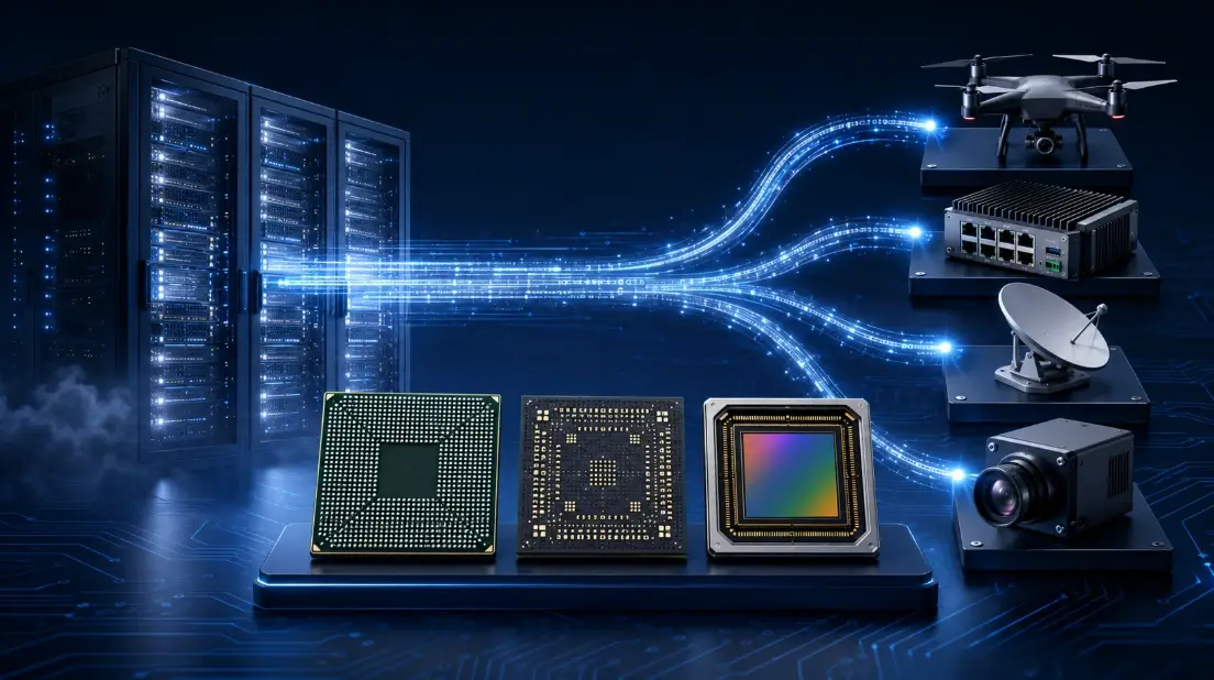
The shift from cloud racks to edge hardware is not only about speed. It is also about data cost, network pressure, local control, and system independence. Cloud computing still matters, but many devices now need to process part of the workload near the source.
In edge AI hardware design, the device often receives data from image sensors, pressure sensors, motion sensors, gas sensors, or communication front ends. A UAV adjusting flight attitude, a machine vision device checking defects, or a satellite terminal handling signal changes cannot treat every decision as a remote cloud task.
That is why Computational Power is moving closer to the sensor and control layer. Local processing helps reduce delay and makes the device less dependent on network stability.
Cloud servers can handle large workloads, but they cannot remove the physical delay of transmission. For real-time control, even small delays can affect system behavior. Bandwidth is also a cost issue. Sending raw video, sensor streams, or RF-related data continuously can create pressure on networks and storage.
Edge hardware does not replace the cloud. It filters, reacts, and sends useful results upward.
A practical edge device usually captures data, processes urgent information locally, and sends processed results to a higher-level system. This reduces unnecessary data transfer and helps the full system run with less communication burden. For buyers, this means the hardware architecture must be planned around data flow, not only processor speed.
Cloud equipment has more space, stronger cooling conditions, a larger power budget, and easier maintenance access. Edge hardware is different. It may be installed inside a compact module, a moving platform, an outdoor unit, or a high-density communication box. This makes substrate choice, sensing design, routing, and package materials more important.
As devices get smaller, the same board area must carry computing, memory, sensing, and communication functions. A standard layout may not provide enough routing space. This is where an advanced IC packaging substrate becomes important, especially for processors that require dense I/O and short signal paths.
Edge hardware designers often face several problems at once. Higher computing density can increase heat. Smaller boards make routing harder. Fast signals need cleaner paths. Mechanical vibration or outdoor use can add extra risk.
A common mistake is treating these as separate issues. In real projects, substrate structure, package material, sensor placement, and thermal paths affect each other.
Engineering Notice and Material Boundaries: When computational workloads move into tight edge modules, thermal expansion mismatch becomes one of the first failure risks to review. For IC packaging substrates, the CTE window should be checked together with the processor package, PCB, solder joint structure, and final enclosure. DEEPETCH’s FCBGA roadmap includes CTE ranges moving from 7.2–9.5 ppm toward lower windows such as 5.6–8 ppm and 3–4 ppm in later material directions. It also lists fine Line/Space capability such as 9/12 μm and 8/8 μm, with μbump pitch moving from 110 μm toward 90 μm. For high-density chip packaging, these boundaries are not decorative data. They affect impedance control, parasitic capacitance, microvia reliability, and local heat concentration. Buyers should also request project-specific dielectric constant and dissipation factor data during early layout review, instead of assuming that one substrate material fits every edge AI or RF module.
Edge systems may work near motors, antennas, batteries, optical paths, or outdoor equipment. Vibration, temperature change, humidity, and electromagnetic interference may be normal operating conditions. Buyers should consider not only performance claims, but also where the module will be used and how the structure will be tested.
As Computational Power moves into smaller devices, chip packaging becomes a central design topic. The package substrate connects the processor to the board while supporting dense routing and stable signal transmission. For edge AI modules, 6G communication hardware, UAV control systems, and satellite communication electronics, this is part of the core design, not a secondary detail.
FCBGA Substrate fits projects that need high-density chip packaging for processors or advanced computing devices. It helps connect the chip to the system board while supporting compact routing requirements.
For buyers, the key question is not only whether the substrate can support the chip. The better question is whether it can support the full product structure after layout, assembly, thermal review, and reliability checking.
More compact computing hardware often moves toward advanced packaging ideas, such as tighter stack-up planning and multi-die integration. FCBGA Substrate is relevant here because it supports shorter interconnect paths and more integrated package structures.
This product is more suitable for high-value modules than simple low-density boards. It fits projects where the chip package affects the final system size and signal behavior.
Choose FCBGA Substrate when your project involves edge AI processors, 6G-related hardware, UAV control electronics, or satellite communication processing boards. It is especially suitable when board space is limited but computing and signal requirements are high.
Computing at the edge starts with sensing. If the input signal is unstable, late, noisy, or poorly calibrated, the processor cannot make good decisions. Sensor products should be considered early in system planning, not added after the main board structure is already fixed.
Sensor chip series is relevant because sensors are the first layer of real-world data. The product direction can connect with photoelectric sensing, MEMS sensor chips, CMOS image sensing, LiDAR sensing, and ambient light sensing.
For drones, smart inspection devices, industrial vision, and environmental monitoring, custom sensor chip solutions can help match the signal source to the actual working environment.
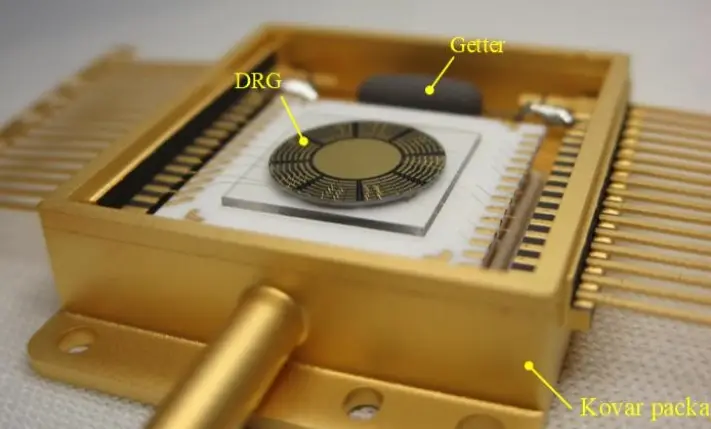
Motion and vision systems need fast input. A vision device may need to detect defects on a moving line. A UAV may need to respond to movement, angle, or environmental changes. A smart terminal may need to process optical or distance-related information without waiting for cloud feedback.
Here, Computational Power only works well when sensing and processing are planned together.
Choose Sensor chip series when the project depends on accurate data capture. It is a natural match for edge systems that use image sensing, position sensing, light sensing, pressure sensing, or environmental sensing before local processing.
When more functions enter a smaller package, the build-up material matters. ABF substrate supports advanced packaging by helping create finer interconnection structures in compact packages. It is not always visible in the final product, but it can affect routing density, manufacturing consistency, and package behavior.
ABF substrate is suitable for advanced package structures where density is a major concern. In edge computing hardware, this matters because the device must often carry computing, storage, sensing, and communication paths in a limited footprint.
Compared with basic board-level thinking, ABF substrate belongs closer to the packaging layer. It supports the compacting of Computational Power before the device reaches final PCBA assembly.
For high-density packages, material behavior during lamination, curing, drilling, and build-up processing affects final consistency. A substrate material must match the process flow. Poor material selection can lead to warpage, registration problems, or reliability risks during later assembly.
This is why buyers should discuss package structure, stack-up, and manufacturing path before deciding only by price.
Choose ABF substrate when the project involves advanced IC packaging, compact processor modules, or packaging structures where fine routing and stable build-up layers matter. It pairs naturally with FCBGA-related projects.
A good sourcing decision starts from the device function, not from the catalog. Buyers should first define what the edge hardware must do locally, what data it must collect, what signals it must transmit, and how much space the final module allows.
| Project Need | Recommended DEEPETCH Product | Procurement Logic |
|---|---|---|
| Compact processor packaging | FCBGA Substrate | Use when computing density and package routing are central |
| Real-world data acquisition | Sensor chip series | Use when sensing accuracy and application matching matter |
| Advanced package build-up | ABF substrate | Use when fine interconnection and compact packaging are needed |
If the main challenge is placing stronger computing capability into a smaller module, FCBGA Substrate should be reviewed early. It is suitable for projects where the processor package affects the whole system design.
If the edge device depends on camera, LiDAR, MEMS, light, pressure, or environmental input, Sensor chip series should be considered with the system architecture. Sensor selection affects data quality before any algorithm runs.
If the project uses dense package structures, ABF substrate can support the packaging foundation. It is especially relevant when Computational Power must fit into a small footprint without treating the substrate as an afterthought.
For edge hardware projects, the difficult part is often not naming a product, but matching substrate, sensor, package structure, and application environment. If your team is comparing package routes, checking sensor options, or preparing purchase details for a compact computing module, share the working conditions, target device size, and expected function list through DEEPETCH contact. That helps the technical discussion stay focused on real project constraints.
Q: Why Is Computational Power Moving to Edge Hardware?
A: Computational Power is moving to edge hardware because many devices need faster local response, lower data traffic, and less dependence on constant cloud connection. Edge devices can process urgent data near sensors and send only useful results upward.
Q: Is FCBGA Substrate Suitable for Edge AI Hardware?
A: Yes. FCBGA Substrate is suitable when edge AI hardware needs compact processor packaging, dense interconnection, and better support for complex chip structures. It is more relevant for advanced modules than simple low-density boards.
Q: How Do Sensor Chips Affect Edge Computing Performance?
A: Sensor chips affect the quality of input data. If sensing is unstable or poorly matched to the application, local processing will not solve the problem. For edge systems, sensor selection and computing design should be planned together.

The DE-CW-1310 DFB EPI wafer, a high-performance epitaxial structure designed for distributed feedback (DFB) lasers operating at 1310 nm....

Ceramic thin-filmvacuum sensor Optical gas massflowmeter Liquid mass flowmeter Force sensor MEMS...

Photoelectric sensing chip Light source chips Optical transmission and modulationchips Optical detection and receptionchips...

Using a“Detach Core”which has two-layers carrier foil structure on the surface as a core, and forming...

Tenting process is a kind of subtractive process, the process as follows: Laminating photosensitive film...

Modified Semi-Added Process abbreviated as mSAP, which can be used on the core or build-up layers, pattern...

Semi-Added Process abbreviated as SAP, using on the build-up-layer pattern forming as follow:First depositing...

The product generally adopts the pressing lamination process of semi-curing sheets , and line formation...

The products generally adopt the Build-up Film Lamination process, and the circuit formation uses the...
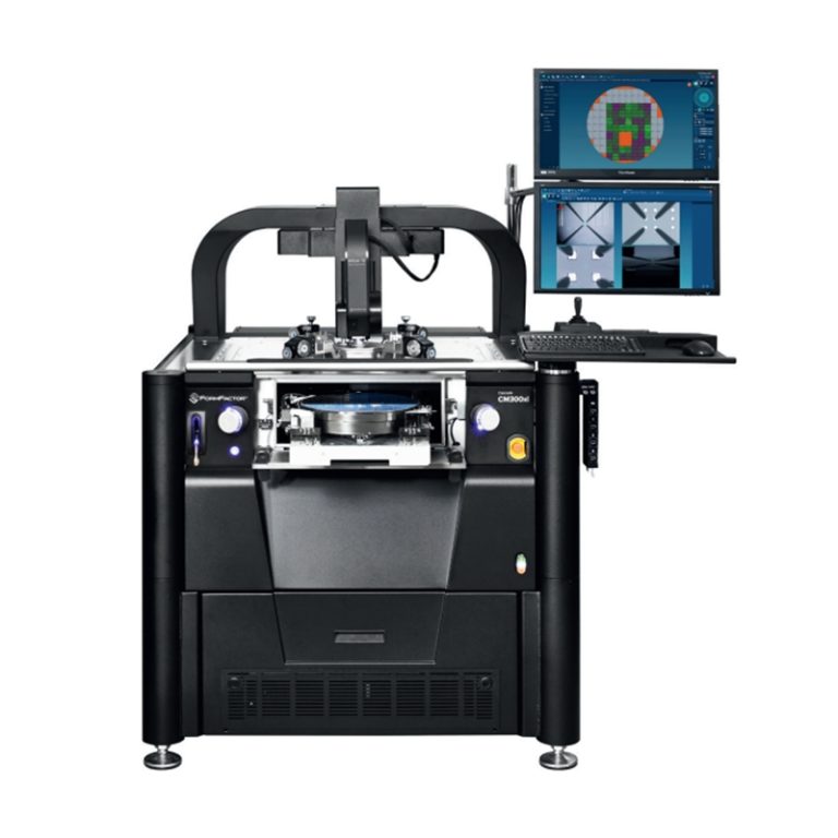
Equipment features: 1. Non-destructive precision testing Micrometer-level probe contact technology...