
UV Debonding Film

The DEEPETCH UV Debonding Film is a core supporting material engineered for advanced semiconductor wafer processing. Designed to protect wafers during dicing and back-end packaging, this film features an ultra-thin 50-100μm profile with excellent flexibility. Through its proprietary UV-responsive pressure-sensitive adhesive, the film exhibits a massive 90% drop in adhesion after UV irradiation, allowing for clean, damage-free peeling. With exceptional cutting resistance and low-residue formulation, it is a critical material for high-precision wafer dicing, MEMS, and advanced packaging applications.

UV Debonding Film-1

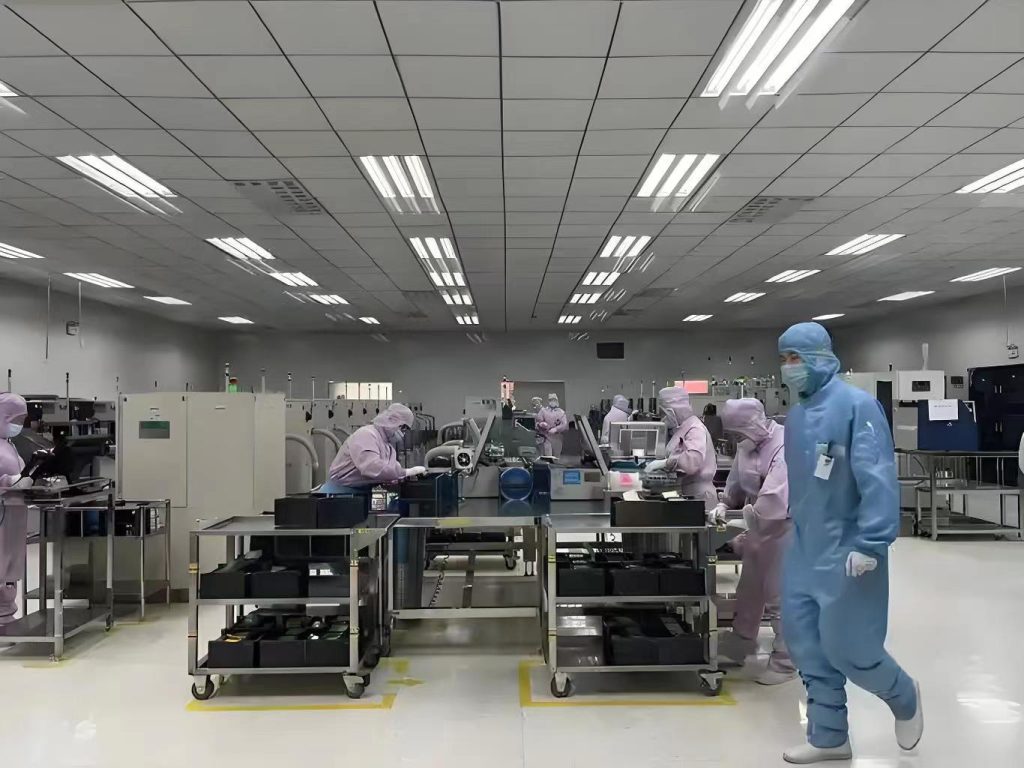
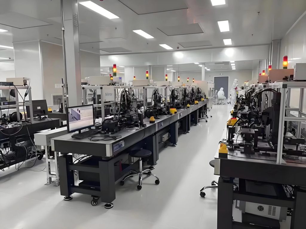
Product album display

Engineering Application Technology

  • Ultra-Thin Substrate & Precision Coating: Ensures excellent flexibility and adhesion. The film perfectly conforms to different wafer sizes with no bubbles or wrinkles, providing a flat foundation for subsequent processes (Thickness: 50-100μm).

  • Low Residue & Clean Peeling: By optimizing the adhesive molecular structure and cross-linking density, a stable 3D network is formed after UV curing. This prevents small molecule residues, achieving a 90% decrease in adhesion for clean peeling.


Formulation Technology

  • UV-Responsive Pressure-Sensitive Adhesive: Self-developed UV-curable PSA system. By precisely adjusting the ratio of prepolymers, monomers, and photoinitiators, it achieves a massive difference in adhesion before and after light exposure.

  • Dicing & Process Compatibility: The adhesive formula features excellent cutting resistance, easily withstanding the stress of high-speed rotating dicing blades to prevent adhesive tearing or debris generation.


Technical Parameters & Processes

Lithography Type Wavelength Resolution Application Field
UV Broadband Photoresist 300 ~ 450 nm > 2 μm Discrete Devices, MEMS, Packaging
G-line Photoresist 436 nm 0.5 μm and above LCD, LED, Mid-to-low-end ICs
I-line Photoresist 365 nm 0.35 ~ 0.25 μm Non-critical layers of PCB ICs, Thick film passivation
KrF Photoresist 248 nm 0.13 ~ 0.11 μm Process chips above 0.25μm
ArF Photoresist (Immersion) 193 nm 45 ~ 7 nm High-end semiconductors (e.g., 7nm node)
EUV Photoresist 13.5 nm < 7 nm Advanced processes below 5nm
chip

Application Areas

The DEEPETCH UV Debonding Film is designed to support a wide range of semiconductor manufacturing processes (as detailed in the process application matrix):

  • Discrete Devices, MEMS & Packaging: Providing reliable temporary bonding for micro-electromechanical systems and various packaging processes.

  • Optoelectronics: Supporting the manufacturing of LCD, LED, and mid-to-low-end integrated circuits (e.g., G-line lithography applications).

  • PCB & Integrated Circuits: Serving as a protective carrier film for non-critical layers of PCB ICs and thick film passivation processes (I-line applications).

  • Advanced Semiconductor Nodes: Compatible with the stringent requirements of high-end semiconductor manufacturing, including 0.25μm process chips (KrF), 7nm node devices (ArF immersion), and advanced processes below 5nm (EUV).

IDM Customization Service

From advanced processes to specialty processes, we use our IDM vertical integration experience to help customers overcome design-process collaboration challenges.

01

Supports advanced nodes such as [5-22nm FinFET/BCD/GAA] to meet the needs of high-performance computing (HPC), AI chips, etc.

02

MPW (Multi-Project Wafer) Service: Small batch trial production to reduce customers' initial costs. Customized process development: Cooperate with customers to conduct DTCO (Design-Process Co-Optimization), customize design rules and process parameters.

03

We support the joint solution of "wafer foundry + advanced packaging" (such as 3D IC, heterogeneous integration) to avoid the loss of multi-supplier collaboration. Unlike pure foundries, we verify the process stability through mass production of our own chips to reduce the risk of tape-out for you.

Provide customers with complete integrated manufacturing services from concept to finished product

01

Electronic manufacturing services and printed circuit board assembly.

02

EMS provides a wide range of electronic manufacturing services, including everything from circuit board design to supply chain management to assembly, testing and after-sales support.

03

PCBA is a link in EMS that focuses on the assembly of printed circuit boards, covering component placement, soldering and related testing, connecting electronic components to manufactured printed circuit boards.

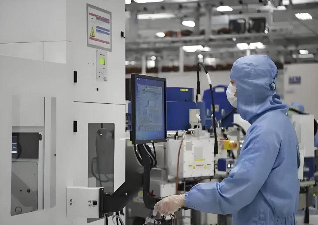
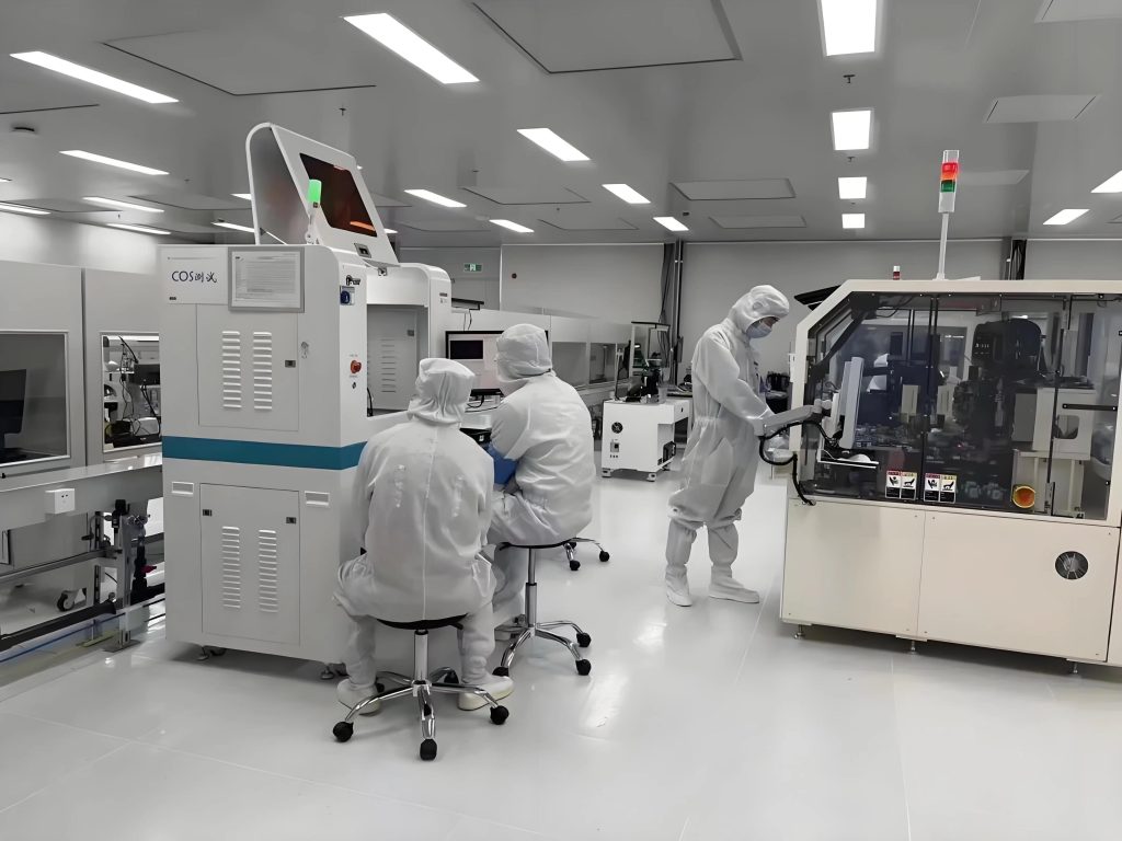
Semiconductor production shop environment

News Center