
The DEEPETCH UV Debonding Film is a core supporting material engineered for advanced semiconductor wafer processing. Designed to protect wafers during dicing and back-end packaging, this film features an ultra-thin 50-100μm profile with excellent flexibility. Through its proprietary UV-responsive pressure-sensitive adhesive, the film exhibits a massive 90% drop in adhesion after UV irradiation, allowing for clean, damage-free peeling. With exceptional cutting resistance and low-residue formulation, it is a critical material for high-precision wafer dicing, MEMS, and advanced packaging applications.
Ultra-Thin Substrate & Precision Coating: Ensures excellent flexibility and adhesion. The film perfectly conforms to different wafer sizes with no bubbles or wrinkles, providing a flat foundation for subsequent processes (Thickness: 50-100μm).
Low Residue & Clean Peeling: By optimizing the adhesive molecular structure and cross-linking density, a stable 3D network is formed after UV curing. This prevents small molecule residues, achieving a 90% decrease in adhesion for clean peeling.
UV-Responsive Pressure-Sensitive Adhesive: Self-developed UV-curable PSA system. By precisely adjusting the ratio of prepolymers, monomers, and photoinitiators, it achieves a massive difference in adhesion before and after light exposure.
Dicing & Process Compatibility: The adhesive formula features excellent cutting resistance, easily withstanding the stress of high-speed rotating dicing blades to prevent adhesive tearing or debris generation.
| Lithography Type | Wavelength | Resolution | Application Field |
|---|---|---|---|
| UV Broadband Photoresist | 300 ~ 450 nm | > 2 μm | Discrete Devices, MEMS, Packaging |
| G-line Photoresist | 436 nm | 0.5 μm and above | LCD, LED, Mid-to-low-end ICs |
| I-line Photoresist | 365 nm | 0.35 ~ 0.25 μm | Non-critical layers of PCB ICs, Thick film passivation |
| KrF Photoresist | 248 nm | 0.13 ~ 0.11 μm | Process chips above 0.25μm |
| ArF Photoresist (Immersion) | 193 nm | 45 ~ 7 nm | High-end semiconductors (e.g., 7nm node) |
| EUV Photoresist | 13.5 nm | < 7 nm | Advanced processes below 5nm |
The DEEPETCH UV Debonding Film is designed to support a wide range of semiconductor manufacturing processes (as detailed in the process application matrix):
Discrete Devices, MEMS & Packaging: Providing reliable temporary bonding for micro-electromechanical systems and various packaging processes.
Optoelectronics: Supporting the manufacturing of LCD, LED, and mid-to-low-end integrated circuits (e.g., G-line lithography applications).
PCB & Integrated Circuits: Serving as a protective carrier film for non-critical layers of PCB ICs and thick film passivation processes (I-line applications).
Advanced Semiconductor Nodes: Compatible with the stringent requirements of high-end semiconductor manufacturing, including 0.25μm process chips (KrF), 7nm node devices (ArF immersion), and advanced processes below 5nm (EUV).
The DEEPETCH UV Debonding Film is a core supporting material engineered for advanced semiconductor wafer...
The SCH Series is a high-performance DAF/DDAF (Die Attach Film) designed to streamline and enhance the advanced packaging process....
The DEEPETCH DP-QPA2611 is a high-performance X-Band (8–12 GHz) Gallium Nitride (GaN) Power Amplifier...
The DEEPETCH DP-ROS-40121 is a premium, solvent-free epoxy die attach adhesive engineered for the most...
The Diamond Heat Spreader is a highly efficient thermal management material engineered for the most demanding...
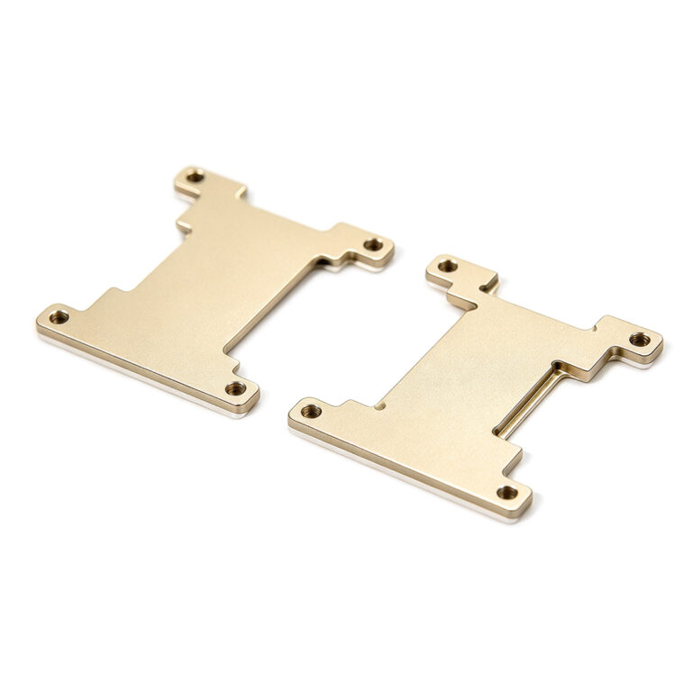
Molybdenum copper composite: adjustable CTE, high conductivity, lower density than tungsten copper. No...
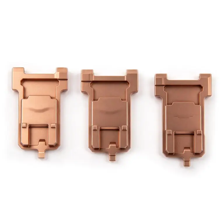
Tungsten copper composite: low CTE, high conductivity. Ideal for RF, power, optical packaging.
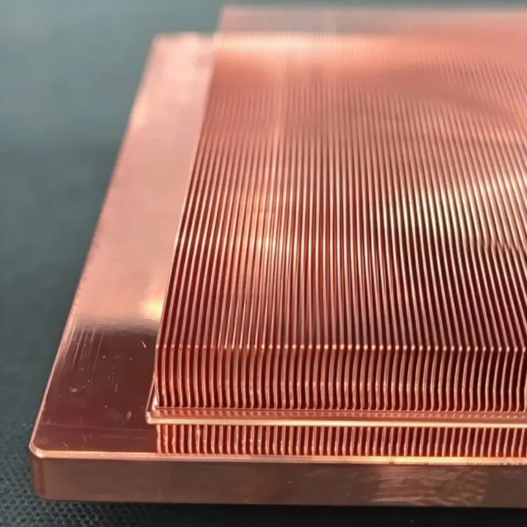
Diamond-Copper Thermally Conductive Composite. High thermal conductivity, tunable CTE, robust.
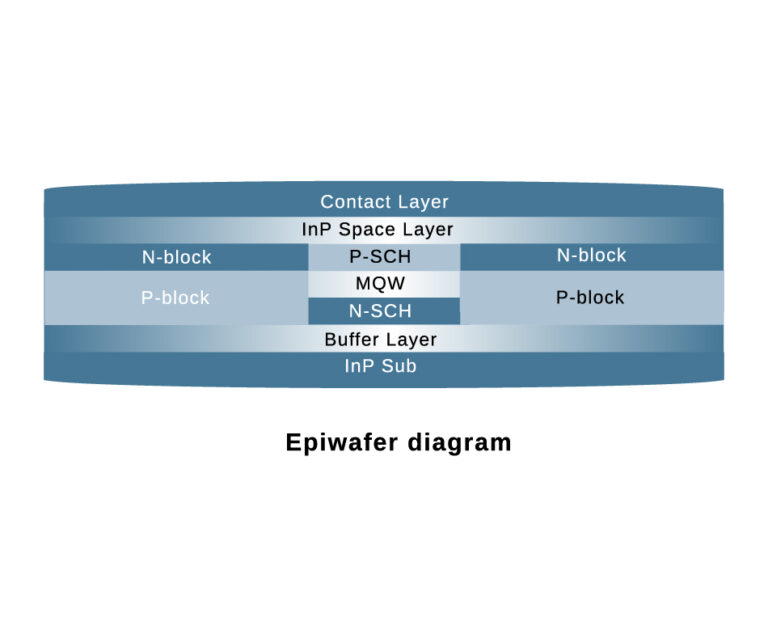
The DE-CW-1310 DFB EPI wafer, a high-performance epitaxial structure designed for distributed feedback (DFB) lasers operating at 1310 nm....
Ceramic thin-filmvacuum sensor Optical gas massflowmeter Liquid mass flowmeter Force sensor MEMS...
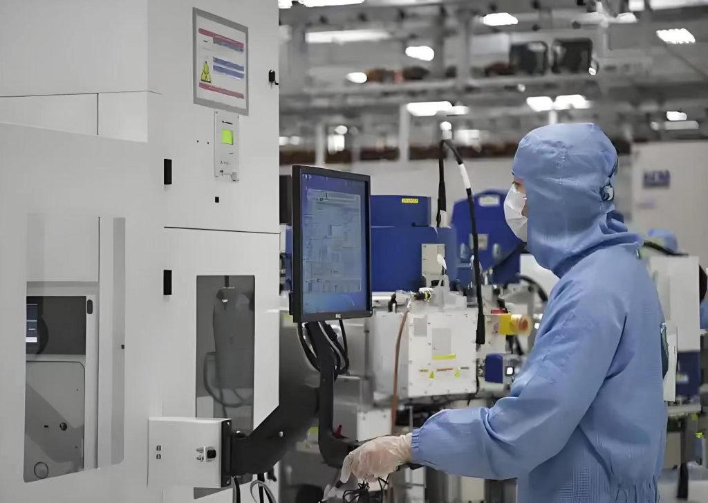
Supports advanced nodes such as [5-22nm FinFET/BCD/GAA] to meet the needs of high-performance computing (HPC), AI chips, etc.
MPW (Multi-Project Wafer) Service: Small batch trial production to reduce customers' initial costs. Customized process development: Cooperate with customers to conduct DTCO (Design-Process Co-Optimization), customize design rules and process parameters.
We support the joint solution of "wafer foundry + advanced packaging" (such as 3D IC, heterogeneous integration) to avoid the loss of multi-supplier collaboration. Unlike pure foundries, we verify the process stability through mass production of our own chips to reduce the risk of tape-out for you.
Electronic manufacturing services and printed circuit board assembly.
EMS provides a wide range of electronic manufacturing services, including everything from circuit board design to supply chain management to assembly, testing and after-sales support.
PCBA is a link in EMS that focuses on the assembly of printed circuit boards, covering component placement, soldering and related testing, connecting electronic components to manufactured printed circuit boards.
Title: Semiconductor manufacturing processes Objective: To have a certain foundation for the overall...