

Coreless substrate manufacturing still begins on support. The support simply leaves before shipment. First copper sits on a detachable carrier; dielectric and later copper grow around it. Then comes the awkward moment: release. A panel that looked flat on its carrier can spring, twist or pick up edge damage once that restraint disappears.
DEEPETCH supplies semiconductor materials, process equipment and packaging-related products, with coreless process and FCCSP substrate options in its portfolio. Buyers tend to ask about line formation first. A harder question is what happens to that line afterward. Can the factory keep it registered and protected through lamination, separation and the last surface steps?
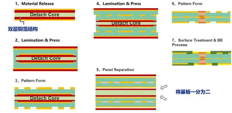
Think of the temporary core as shop-floor tooling. It steadies the first build-up layers during imaging, plating, lamination and handling, then goes away. A finished-stack drawing rarely shows that working history, so several important choices vanish from the buyer’s view.
For an ETS coreless substrate, the factory makes the first circuit on copper foil carried by the detachable core. Prepreg closes around the pattern during lamination. After separation, etching removes the exposed surface copper and the trace remains set into the dielectric. Put this ETS coreless substrate sequence on the process flow. “Coreless build-up” by itself says too little.
That sequence changes how the first layer should be reviewed. The buyer should identify which face begins on the carrier, which copper becomes the embedded trace and which surface is exposed after release. Without that orientation, a supplier can follow the layer count and still interpret the build direction differently.
The DEEPETCH Coreless Process shows this build-up and separation route. Use it as a process map when discussing the detach core process, then add the actual layer naming, finished-side orientation and inspection points for the project.
On a flow chart, release may be one arrow between lamination and finishing. On the floor, it is the instant when mechanical support changes hands. The carrier had been holding the panel; the thin build-up must now carry whatever stress the earlier steps left behind.
For that reason, the detach core process needs acceptance checks before and after release. Compare panel condition, visible damage, dimensional registration and bow at the same reference points. A pass before release does not prove that the released panel is ready for the next operation.
Coreless substrate manufacturing becomes easier to control when each stage has a named purpose. The sequence below is more useful for an RFQ than a single label such as coreless build-up.
The first pattern is created on the copper foil of the detachable structure. Its position sets the reference for later layers, so artwork orientation and panel datum should be settled before tooling. Once prepreg surrounds the pattern, that copper is no longer handled like an exposed outer layer.
That is the working idea behind embedded trace substrate manufacturing. Dielectric closes around the circuit instead of leaving all first-layer copper proud of the surface. There is little room to undo an early particle, damaged pattern or registration miss once the layer is buried.
During lamination, the detach core still holds the work while dielectric and copper are added. Review the two sides together. Pressing and cooling do not care that the purchasing drawing was split into separate layer notes; copper spread, dielectric placement and build order act as one mechanical system.
A final thickness target is not enough. Ask how each side is checked before release and how the panel keeps its orientation from imaging to lamination. If a later map moves, embedded trace substrate manufacturing records can show whether the pattern moved first or the laminated build did.
After build-up, the two sides are separated from the temporary core. Surface copper is then etched to reveal the embedded trace layer, followed by the remaining surface and back-end operations required by the product route.
This point in coreless substrate manufacturing deserves its own traveler entry. Record the panel identity, release side, observed edge condition and any hold time before subsequent processing. The released structure is more sensitive to handling, and an unlabeled wait can make a later shape change hard to trace.
Without a permanent core, the finished structure has less stiffness to mask build imbalance. Coreless substrate warpage control begins while the panel is still attached. Waiting for final inspection is waiting until the evidence has blurred.
Few functional designs are perfectly mirrored. That is acceptable if the team knows where the imbalance sits. Dense copper on one side, a different dielectric build on the other, or a large open patch can make the two faces shrink and relax differently.
Have the supplier check copper by functional region as well as by panel average. Total coverage can look tidy even when a power area is crowded and its neighbor is nearly empty. The carrier may hide that contrast; the released panel will not.
One final bow value says little about when the change occurred. For coreless substrate warpage control, use at least a pre-release and post-release comparison, with the measurement orientation stated. If later thermal or surface steps are expected to move the panel again, add another checkpoint after those operations.
The measurement plan should also match how the substrate will be handled. A free-state panel, a vacuum-held panel and a singulated unit do not present the same shape. Name the condition instead of writing only “warpage inspection.”
The useful comparison is not simply thin versus thick. A core changes the mechanical reference, drilling route, build symmetry and the way accumulated stress is carried. The package design should determine which trade is acceptable.
A coreless route leaves no permanent central core and can suit a thin stack or routing built around ETS. The trade is plain: handling and flatness become daily process concerns rather than end-of-line checks.
For a coreless substrate vs cored substrate review, lay the final cross-sections beside the manufacturing plans. Panel format, unit size, copper spread, assembly heat, temporary support and post-release metrology often settle the choice before a nominal thickness does.
An FCCSP program may use mSAP or ETS-related construction depending on the design and supplier route. The DEEPETCH FCCSP Substrate is relevant when the package needs a fine interconnect substrate and the construction is being selected with the application in mind.
Do not put “FCCSP” in an RFQ and assume the build is settled. State whether the expected route is cored, coreless or still open, and attach the layer stack. The coreless substrate vs cored substrate decision should be visible before the supplier commits tooling and inspection planning.

Write the coreless substrate manufacturing RFQ like a short traveler. Leave recipe ownership with the factory, but show the build, its orientation and the rule for accepting a released panel. The useful record is not just “passed.” It shows whether anything moved at release and what passed at delivery.
| RFQ field | What to state | Why it matters |
| Build orientation | Carrier-side layer, release face and finished-side naming | Prevents an inverted stack interpretation |
| Panel and unit | Panel format, unit outline and handling edge | Connects processing to mechanical support |
| First pattern | Copper role, datum and embedded-trace intent | Fixes the reference for later registration |
| Stack | Copper and dielectric sequence on both sides | Exposes build imbalance before lamination |
| Release | Separation point and checks before and after release | Makes the temporary-support handoff auditable |
| Shape control | Measurement state, orientation and checkpoints | Gives warpage results a comparable condition |
| Delivery | Surface finish, singulated or panel state and records | Defines what the assembly line receives |
Request layer registration records, build orientation and the shape checkpoints agreed for the program. If a released panel moves, those records show whether the change followed lamination, separation or a later thermal step. A final certificate alone cannot answer that question.
Also ask how nonconforming units are marked and contained. Thin panels can look acceptable while held by a fixture. The release condition and inspection state should therefore stay attached to the lot history.
Put the intended copper distribution and panel layout into early lots. A simple coupon is fine for material screening, yet it seldom carries the product’s stress balance. Change one item, keep the build order still, and repeat the same measurements on both sides of release.
If the stack orientation, release inspection or warpage checkpoints are still open, share the cross-section and intended delivery state when you contact the DEEPETCH team. That gives the coreless substrate manufacturing discussion a real process object and keeps the first supplier response focused on the unresolved choices.
The factory forms the first circuit on copper foil held by a temporary core. It laminates dielectric and later layers around the pattern, separates the built structure, then etches surface copper until the embedded trace is exposed. The core leaves with the tooling; it does not leave with the substrate.
Release lets stored stress from copper, dielectric, pressing and cooling show itself. An imbalanced panel may move immediately or wait until another hot process. Compare shape at several boundaries and write down whether the panel was free, held or already singulated.
Start with package profile and routing, then test the choice against handling, support, copper balance, assembly heat and available metrology. A design may benefit from losing the permanent core. The factory still has to explain release, flatness and the inspection state used at delivery.

The DEEPETCH UV Debonding Film is a core supporting material engineered for advanced semiconductor wafer...

The SCH Series is a high-performance DAF/DDAF (Die Attach Film) designed to streamline and enhance the advanced packaging process....

The DEEPETCH DP-QPA2611 is a high-performance X-Band (8–12 GHz) Gallium Nitride (GaN) Power Amplifier...

The DEEPETCH DP-ROS-40121 is a premium, solvent-free epoxy die attach adhesive engineered for the most...
The Diamond Heat Spreader is a highly efficient thermal management material engineered for the most demanding...
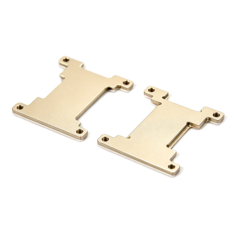
Molybdenum copper composite: adjustable CTE, high conductivity, lower density than tungsten copper. No...
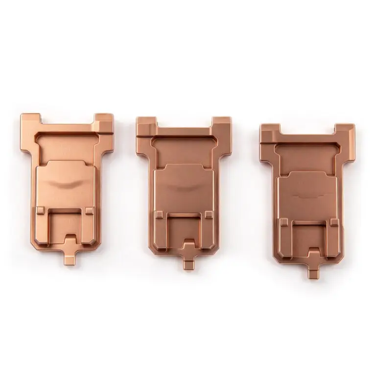
Tungsten copper composite: low CTE, high conductivity. Ideal for RF, power, optical packaging.
Diamond-Copper Thermally Conductive Composite. High thermal conductivity, tunable CTE, robust.
The DE-CW-1310 DFB EPI wafer, a high-performance epitaxial structure designed for distributed feedback (DFB) lasers operating at 1310 nm....
Ceramic thin-filmvacuum sensor Optical gas massflowmeter Liquid mass flowmeter Force sensor MEMS...