

A DFB epitaxial wafer arrives many steps before a working laser. “1310 nm” cannot settle the purchase on its own. The layer stack has to meet a grating route, possible regrowth, ridge etching, metallization and facet work. If those owners make different assumptions, the mismatch usually appears on a processed wafer, after the cheap questions have become expensive ones.
DEEPETCH supplies semiconductor materials and optoelectronic products, including a 1310 nm DFB epi structure for continuous-wave laser development. Start with the route on the fab floor. Where does the grating enter? How will the ridge and current confinement be made? Which test follows the wafer ID through processing? Those answers give the material request a shape.

An epi stack supports a device concept; it does not choose one. Put optics and fabrication on the same cross-section before requesting an InP DFB laser wafer. The DFB epitaxial wafer order can then name an owner for each interface instead of carrying a bundle of unspoken guesses.
On the incoming side, teams may control photoluminescence wavelength and uniformity, layer thickness and doping. On the finished chip, they may watch lasing wavelength, threshold behavior, slope efficiency or output at a stated condition. One set informs the other; neither can stand in for it.
Write the DFB epi wafer specification in two columns. One column contains wafer acceptance fields; the other contains device targets verified after fabrication. This prevents a chip-level objective from being treated as a direct incoming-wafer guarantee.
The DE-CW-1310 DFB EPI Wafer is designed for DFB lasers operating at 1310 nm. Its product page gives a practical list of epitaxy controls and typical chip fields for discussion. Those fields are a starting sheet, not a substitute for the customer’s route and acceptance method.
Every DFB route needs wavelength-selective feedback, but the grating does not enter every flow at the same point. One team may pattern it before a regrowth step; another may use a different sequence suited to its device. The surface and interface requested from the epi supplier change with that choice.
For a 1310 nm DFB epi wafer, write down the grating stage, coupling idea and planned regrowth. If two routes are still alive, say so and review both before the stack freezes. “DFB compatible” leaves the most important interface undefined.
A useful cross-section prompts the next process owner to act. Generic layer names help with orientation. Fabrication still needs the working interfaces and allowable variation tied to its own sequence.
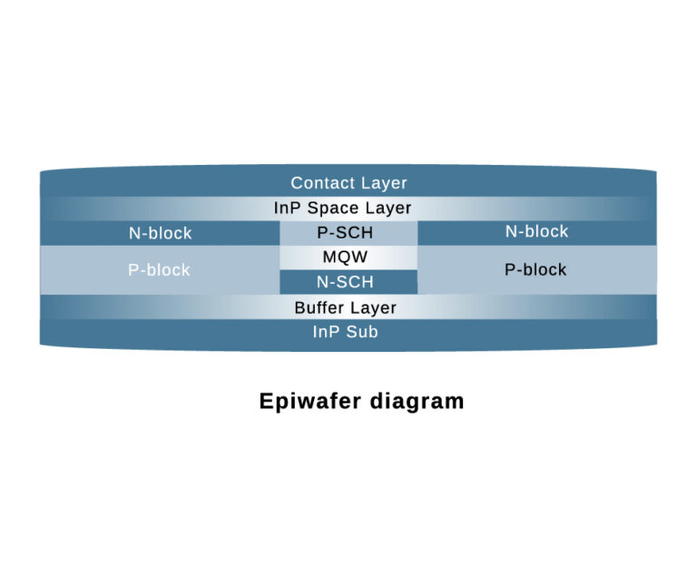
One DFB epitaxial wafer structure can place buffer and separate-confinement layers above an InP substrate, around a multiple-quantum-well region, with blocking, spacing and contact-related layers above. The labels explain optical and electrical jobs. They do not tell the etcher where to stop or the process engineer how deep to cut the ridge.
The chip team should mark the planned etch depth against the supplied layer sequence. It should also identify which layers are exposed during ridge formation and which interface must remain protected for later processing. That is where an InP DFB laser wafer becomes a usable fabrication input rather than a materials diagram.
Doping shapes the electrical path and contact plan. A buyer need not request the grower’s private reactor recipe. The buyer does need to know which doping fields are reported, where they were sampled and how. A lone number with no position can conceal a radial change.
Use a wafer map where uniformity matters. Tie the map orientation to the wafer identification and flat or notch convention used by fabrication. The same reference should follow the wafer through lithography and test so that a device pattern can be compared with the incoming material map.
AI optical interconnect programs ask many optical channels to live inside one manageable assembly and control window. The pressure reaches incoming epi, yet “tight uniformity” is not an inspection plan. First name the field and where it will be measured.
PL wavelength, thickness and doping call for different tools and sampling. Beside each item in the DFB epi wafer specification, write “center,” “radial points,” “map” or the other agreed scheme. Put edge exclusion on the same line; otherwise two maps may look comparable when they cover different usable areas.
The map should answer a process question. If edge chips will be discarded, folding them into one average can skew a supplier comparison. If the fab plans to use the full wafer, a center reading alone may overlook the region that later sets the learning limit.
Lot and wafer identifiers should survive scribing, dicing and test data export. Coordinate orientation before mask layout so that chip coordinates can be traced back to the material map. This is routine discipline, yet it is often lost when separate teams own wafer receiving and device characterization.
For DFB laser chip fabrication, keep the incoming maps beside process deviations and chip coordinates. A wavelength or threshold shift can then be checked against position. Without that thread, every outlier starts another investigation from zero.
The most sensitive handoff may occur after the first epitaxy rather than at goods receipt. Surface condition, time between steps and cleaning decisions can affect what the next growth or patterning operation sees.
State whether the wafer is delivered ready for a grating-related operation, protective handling or another preparation step. Packaging, storage and permitted cleaning should match that state. An aggressive clean chosen by habit may change the surface the regrowth team expected.
In DFB laser chip fabrication, record the time and condition between surface preparation, grating formation and any regrowth. The point is not to force one universal time limit. It is to make the actual handoff visible when comparing lots.
Test structures should resemble the planned grating and ridge route closely enough to reveal real process interactions. A bare monitor can confirm a material step while missing the loading, topography or cleaning behavior of the product pattern.
Use early wafers to close process choices in sequence. Hold the epi design steady while the grating step is tuned, then keep the selected grating route fixed while regrowth or ridge variables are studied. Changing the stack and the downstream process at the same time makes the result difficult to assign.

A DFB wafer for optical interconnects has to fit the assembly, not merely its wavelength label. Coupling, drive, cooling, test access and final placement all push requirements back toward the laser structure.
The chip team needs one agreed operating condition for comparison. Change current, temperature, the thermal path or the fixture and the observed result can move. A tidy supplier table is misleading when its rows came from different test conditions.
For a DFB wafer for optical interconnects, describe the continuous-wave role, temperature setting and coupling path before asking for a device target. If the system is still moving, mark the field open. A made-up number only hides the decision that remains.
InP carries the active laser structure; the finished die may later meet silicon photonics or another optical assembly. Chip outline, facet plan and handling assumptions therefore belong in process development early, even though they are not epitaxy reactor settings.
DEEPETCH also lists Indium phosphide (InP) within its semiconductor material portfolio. When discussing a 1310 nm DFB epi wafer, confirm whether the request is for bare substrate, epitaxial structure or a later chip stage. These are three different deliverables. Giving them one loose specification invites the wrong quotation.
A one-page DFB epitaxial wafer RFQ can save several rounds of email. Mark each field as fixed, awaiting confirmation or checked only after chip fabrication. The supplier can then answer the real gaps instead of restating a catalog description.
| RFQ field | What to state | Decision supported |
| Device role | CW laser use, operating region and optical interface | Connects epi design to the system |
| Fabrication route | Grating stage, regrowth plan, ridge and contact concept | Reveals process compatibility |
| Wafer format | Substrate type, orientation and identification scheme | Aligns handling and traceability |
| Epi acceptance | PL, thickness, doping and agreed sampling fields | Defines incoming inspection |
| Mapping | Measurement locations, edge treatment and map orientation | Makes uniformity comparable |
| Chip validation | Test condition and fields checked after fabrication | Separates material from device acceptance |
| Delivery | Surface state, packaging and storage handoff | Protects the next process step |
Blank cells invite assumptions. Put the current working answer in the cell, name its owner and say when it becomes binding. Grating and regrowth details deserve this treatment because a modest route change can alter the requested surface or layer sequence.
Normalize supplier responses before ranking them. Confirm that each proposal refers to the same wafer state, sampling plan and chip test condition. Separate included mapping from optional characterization, and make sure lot traceability survives the handoff to the fab.
If the grating sequence, map or chip acceptance method is still open, attach the proposed cross-section when you contact the DEEPETCH team. The DFB epitaxial wafer discussion can then settle interfaces before anyone turns an unfinished design into a price request.
List the device role, substrate and orientation, layer structure, grating and regrowth route, incoming epi checks, map reference, delivered surface and later chip tests. Put wafer acceptance and finished-device performance in separate sections.
No. PL is one incoming-material signal. The order also has to align layer design, thickness and doping controls, mapping, grating work, ridge and contact processing, plus the test condition used on fabricated lasers.
It supplies the active and confinement structure from which the laser chip is fabricated. Its value depends on compatibility with the grating, regrowth, ridge, metallization, facet and assembly plan. Traceable maps help the team relate incoming material variation to later chip behavior.

The DEEPETCH UV Debonding Film is a core supporting material engineered for advanced semiconductor wafer...

The SCH Series is a high-performance DAF/DDAF (Die Attach Film) designed to streamline and enhance the advanced packaging process....

The DEEPETCH DP-QPA2611 is a high-performance X-Band (8–12 GHz) Gallium Nitride (GaN) Power Amplifier...

The DEEPETCH DP-ROS-40121 is a premium, solvent-free epoxy die attach adhesive engineered for the most...
The Diamond Heat Spreader is a highly efficient thermal management material engineered for the most demanding...
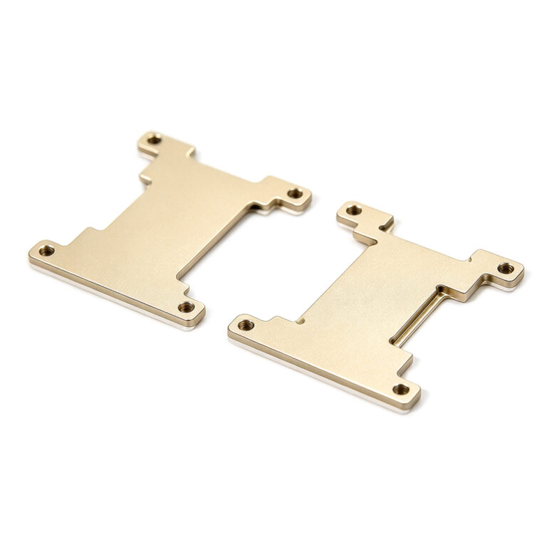
Molybdenum copper composite: adjustable CTE, high conductivity, lower density than tungsten copper. No...
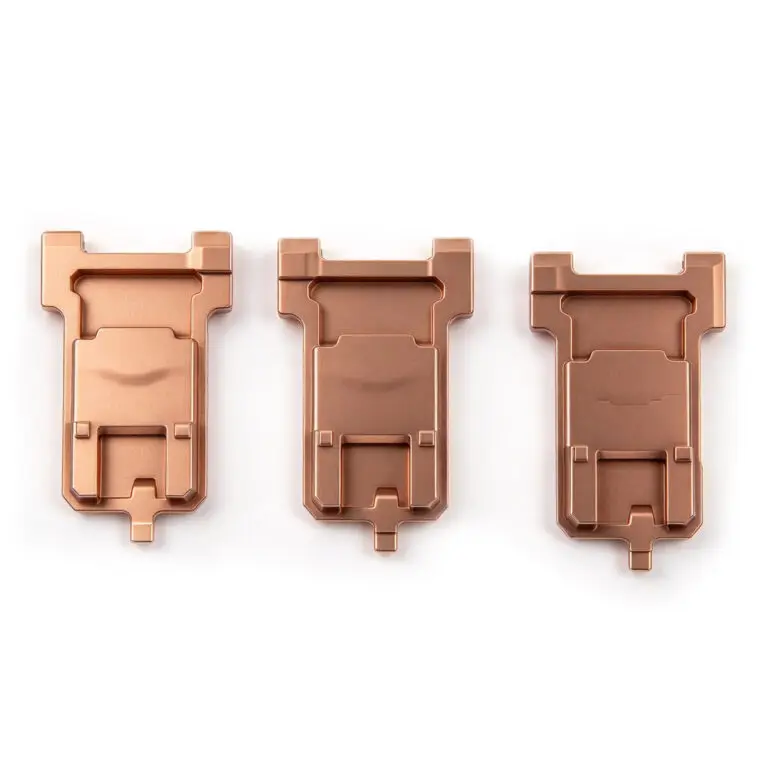
Tungsten copper composite: low CTE, high conductivity. Ideal for RF, power, optical packaging.
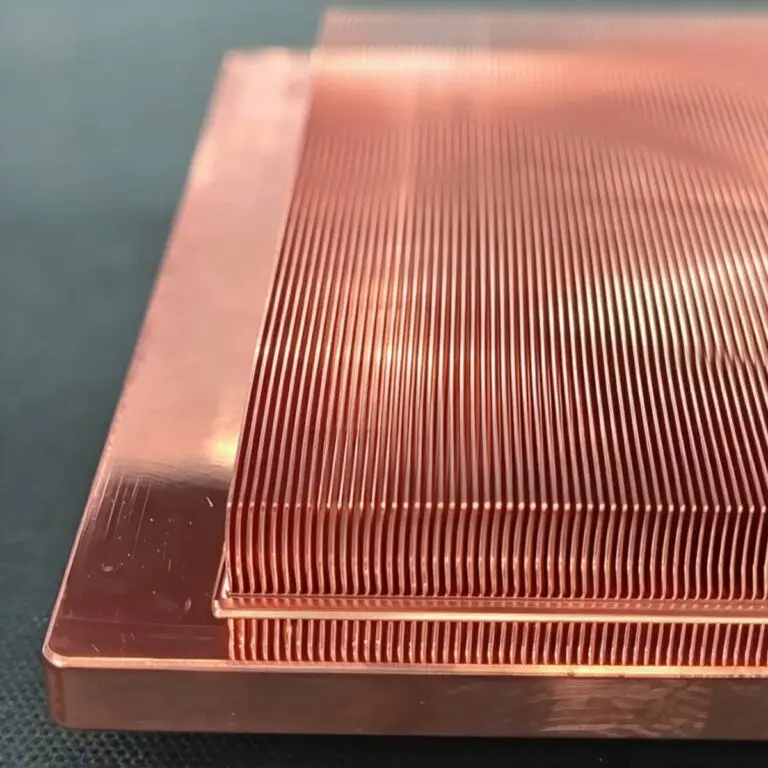
Diamond-Copper Thermally Conductive Composite. High thermal conductivity, tunable CTE, robust.
The DE-CW-1310 DFB EPI wafer, a high-performance epitaxial structure designed for distributed feedback (DFB) lasers operating at 1310 nm....
Ceramic thin-filmvacuum sensor Optical gas massflowmeter Liquid mass flowmeter Force sensor MEMS...