
A modern IC Substrate for 6G hardware is no longer just a passive carrier between the die and the PCB. It has to manage fine-pitch connections, dense routing, signal isolation, thermal paths, and later module assembly. As communication hardware moves toward higher frequency and smaller size, the interposer becomes a practical bridge between advanced chips and manufacturable package structures.
DEEPETCH works across semiconductor materials, IC packaging substrates, ceramic packages, equipment, sensor chip series, and high-speed communication products. For this topic, the most relevant products are FCBGA Substrate and ABF substrate. They fit projects where engineers need compact routing, advanced package integration, and better preparation for PCBA or EMS-level manufacturing.

6G hardware will place more pressure on package design than many current communication products. Higher frequency, shorter signal paths, mixed RF and digital functions, and compact module layouts all make substrate selection more difficult. A standard package carrier may still work for simple devices, but it can become a bottleneck when several functional dies need to communicate inside a small package.
At higher frequencies, routing is not just about connection. It affects loss, delay, impedance control, and noise coupling. A long or poorly controlled path inside the package may weaken the signal before the PCB design even begins.
In 6G hardware packaging, the interposer helps shorten critical paths between dies. It gives engineers more freedom to arrange signal routes before they reach the package substrate. This is especially useful when the module needs fast data movement between RF, logic, memory, or control sections.
Modern communication hardware often combines more functions in one package. A processor die, RF section, memory interface, power management area, and control logic may all compete for routing space. If every signal must go directly through the substrate, the design can become difficult to manufacture.
Interposer-based packaging helps redistribute fine chip-level connections into a more workable layout. It reduces the routing burden on the substrate and gives the package more room for multi-die integration.
Small modules are harder to cool and harder to assemble. Dense interconnects, package warpage, solder joint stress, and heat concentration can all affect product stability.
For buyers, the key is not only whether a substrate can route enough signals. The better question is whether the full package structure can support electrical behavior, thermal transfer, and assembly control at the same time.
An interposer is a transition layer between the die and the package substrate. It helps convert very fine chip-side connections into a routing structure that the substrate and later PCB assembly can handle.
Advanced chips often have very fine bump pitch, in some cases shrinking toward 130µm or below, and dense I/O requirements. A standard package substrate cannot always route these ultra-fine line and space dimensions without creating yield pressure. The interposer acts as the bridge, expanding the pitch from the micro-bumps on the die side to the larger C4 bumps on the substrate side. This reduces manufacturing pressure and avoids forcing the package into an overly aggressive layout too early.
For a buyer, this is not just a technical detail. It affects whether the package can move from prototype to stable production without repeated layout changes.
A 6G package may include multiple circuit domains. RF paths need clean isolation. Logic circuits need fast switching. Memory channels need timing stability. Power delivery must avoid injecting noise into sensitive signal areas.
The interposer helps organize these domains before signals reach the main substrate. This can reduce crosstalk risk and make the later board-level layout more manageable.
A weak package layout often pushes problems into the PCBA stage. Engineers may need more PCB layers, longer routing detours, or extra shielding. That can raise cost and delay validation.
A well-planned IC Substrate structure reduces this pressure. It lets the package absorb part of the routing complexity before the assembly reaches the system board.
For this article, the two most suitable DEEPETCH product directions are FCBGA Substrate and ABF substrate. They are not used in the same way, so buyers should match them to package size, die count, routing density, and production stage.
FCBGA Substrate is the first product to review when a design involves larger package size, more I/O, and advanced multi-die structures. It is especially relevant for FCBGA substrate for chiplets because chiplet integration depends on short die-to-die paths and controlled redistribution.
For a 6G baseband processor, high-speed switching chip, or AI-assisted communication module, FCBGA Substrate can help manage dense package routing before the design moves to PCBA integration.
ABF substrate is more suitable when fine routing, multilayer build-up, and stable interconnection are the main concerns. ABF substrate for high-density routing can help reduce layout pressure inside compact package structures.
This product direction fits projects where the package must carry dense signal paths but still keep the final module compact. It is also useful when the design needs a cleaner transition between semiconductor packaging and later custom PCBA manufacturing.
Some projects should not be judged by one material or one package type alone. For a high-speed TR module, the better workflow is to review interposer needs, substrate build-up, signal path length, thermal path, and PCBA interface together.
This is where DEEPETCH’s wider work in high-speed communication products becomes relevant. The company’s experience with optical modules, AOC, DAC, and OEM/ODM/JDM services gives buyers a more complete route from package-level design to module-level manufacturing.

Buyers should avoid choosing only by product name. The right option depends on the package architecture and the later manufacturing path. An early prototype for a UAV communication board will have different thermal and routing priorities compared with future mass production of consumer base stations.
| Selection Question | More Suitable Direction | Practical Reason |
|---|---|---|
| Does the design involve chiplets or multiple dies | FCBGA Substrate | More suitable for larger advanced package integration |
| Is dense build-up routing the main challenge | ABF substrate | Better fit for fine routing and multilayer package structures |
| Will the package connect to a complex PCBA | FCBGA plus EMS review | Helps reduce redesign risk before board assembly |
| Is the module size tightly limited | Stack-up review first | Final choice depends on I/O, heat, and routing density |
FCBGA Substrate becomes more practical when the design has more dies, more signal connections, or a larger package body. It gives engineers more room to manage package-level routing and die-to-die communication.
For projects using multi-die structures or high-speed processing chips, this product should be reviewed early rather than after the PCB layout is already fixed.
ABF substrate is more suitable when the substrate must support fine routing and compact package interconnection. It is often the better direction when package density is the main constraint.
Buyers should ask for stack-up review, routing feasibility, via structure discussion, and manufacturability feedback before confirming the package plan.
Many package problems start at the design stage. If DFM review happens too late, the project may face redesign, assembly instability, or test access problems.
For custom PCBA manufacturing and EMS projects, substrate planning should be connected with prototype goals, inspection needs, reflow behavior, and batch production expectations. DEEPETCH’s IDM service direction can support this type of early-stage technical discussion.
The value of substrate selection becomes clearer when it is linked to the full hardware path. A package that works on paper still has to survive assembly, testing, and field use.
Before selecting FCBGA Substrate or ABF substrate, engineers should review die count, bump pitch, I/O density, layer requirements, thermal route, and package-to-board transition. This helps avoid selecting a substrate that cannot support the actual package structure.
Substrate design affects PCBA assembly. Solder joint layout, warpage risk, reflow profile, inspection access, and signal continuity should be checked together.
This is especially important for compact radio modules, satellite payload electronics, and UAV control boards, where limited space leaves little room for late-stage fixes.
If your project involves dense routing, interposer feasibility, TR module design, or prototype-to-production planning, prepare your block diagram, expected package size, interface requirements, and use environment before supplier communication. DEEPETCH can help review whether FCBGA Substrate, ABF substrate, or a wider EMS path is more suitable. Use the contact channel when you need technical material review, substrate discussion, or project document matching.
A practical IC Substrate plan for 6G hardware starts with the package problem. Interposers help bridge fine-pitch dies, expand routing pitch, separate mixed circuit domains, and reduce board-level layout pressure.
For larger advanced packages and chiplet-related designs, DEEPETCH FCBGA Substrate should be reviewed first. For dense build-up routing and compact package structures, DEEPETCH ABF substrate is a strong candidate. The safer route is to connect substrate selection with interposer review, PCBA assembly, thermal planning, and EMS production flow before prototype release.
Q: What Is the Role of an Interposer in an IC Substrate?
A: An interposer redistributes signals between fine-pitch dies and the package substrate. It helps expand pitch, reduce routing pressure, and make dense package structures easier to manufacture.
Q: Is FCBGA Substrate Better Than ABF substrate for 6G Hardware?
A: Not always. FCBGA Substrate is usually more suitable for larger packages, chiplets, and multi-die structures. ABF substrate is more suitable when fine build-up routing and compact interconnection are the main priorities.
Q: Why Should EMS Requirements Be Reviewed Before Finalizing Substrate Design?
A: Substrate design affects PCBA layout, solder joint behavior, inspection access, thermal transfer, and testing. Early EMS review helps reduce redesign risk before the project moves from prototype to production.

The DE-CW-1310 DFB EPI wafer, a high-performance epitaxial structure designed for distributed feedback (DFB) lasers operating at 1310 nm....

Ceramic thin-filmvacuum sensor Optical gas massflowmeter Liquid mass flowmeter Force sensor MEMS...

Photoelectric sensing chip Light source chips Optical transmission and modulationchips Optical detection and receptionchips...

Using a“Detach Core”which has two-layers carrier foil structure on the surface as a core, and forming...

Tenting process is a kind of subtractive process, the process as follows: Laminating photosensitive film...

Modified Semi-Added Process abbreviated as mSAP, which can be used on the core or build-up layers, pattern...

Semi-Added Process abbreviated as SAP, using on the build-up-layer pattern forming as follow:First depositing...

The product generally adopts the pressing lamination process of semi-curing sheets , and line formation...

The products generally adopt the Build-up Film Lamination process, and the circuit formation uses the...
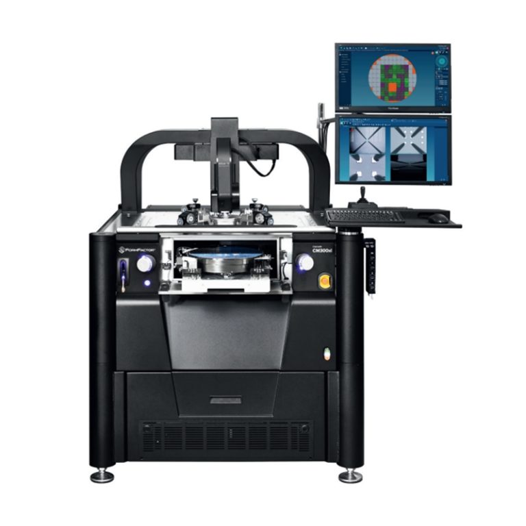
Equipment features: 1. Non-destructive precision testing Micrometer-level probe contact technology...