跳到内容
Products & Service
Wafer raw materials
Substrate material
Ceramic Package
IC packaging substrates
Equipment
Sensor chip series
Silicon wafer
Monocrystalline silicon
Polysilicon
Epitaxial Silicon
Compound semiconductor wafers
Gallium Arsenide (GaAs)
Indium Phosphide (InP)
Gallium Nitride (GaN)
Silicon Carbide (SiC)
Epitaxial Wafer(EPI)
Oxide semiconductor wafer
Zinc Oxide (ZnO)
Indium Tin Oxide (ITO)
Compound Semiconductors
Cadmium Telluride (CdTe)
Aluminum Arsenide (AiAs)
Indium Arsenide (InAs)
Other Materials
Germanium
Silicon-germanium (SiGe)
Graphene
Fourth-generation semiconductor materials
Diamond
Glass
Glass Wafer
Silicon on Insulator
(Soi)
Ceramic Substrate
Alumina
Aluminum Nitride (AIN)
Zirconia
Silicon Nitride
Multilayer ceramic
Inorganic substrate
Glass substrate
Metal substrate
Copper substrate
Aluminum substrate
Organic substrate
FR-4 (glass fiber reinforced epoxy resin)
ABF substrate (Epoxy Deposited Film)
BT resin (bismaleimide triazine resin)
Thermal Management Composites
Diamond Copper Composite (Cu-Diamond)
Ceramic Dual In-line Package (CDIP)
Butterfly Package
Ceramic Quad Flat Package (CQFP)
Ceramic Pin Grid Array Package (CPGA)
Ceramic Small Outline Package (CSOP)
Ceramic Leadless Chip Carrier Package (CLCC)
Ceramic Ball Array (CBGA)
Ceramic SOP
Ceramic DIP
Ceramic QFP
FCBGA Substrate
FCCSP Substrate
SAP Process
mSAP Process
Tenting process
Coreless Process
Maskless Lithography/LDI-laser direct imager
Mask Aligner
Wet etching equipment
ICP RIE System (III-V and Metal Etching)
Deep RIE System (SiOx, SiNx and Deep Si Etching)
PECVD (Plasma Enhanced Vapour Deposition System andGas System for Etching&PECVD Systems
Optical Microscopes
DC–RF Sputter System
E-beam Evaporation System
ALD System (Atomic Layer Deposition)
Automatic Dicing Saw Machine
Oxygen Plasma System
Probe station
AOI test equipment
Ellipsometers
Reflectometer
Packaging equipment
X-RAY testing equipment
X-RAY point equipment
Electroplating equipment
Glovebox System
High temperature furnace
Vacuum furnace
Tunnel furnace
Rapid Thermal Annealer
Wafer polishing equipment
Wafer thinning device
Raman Microscope and Spectrometer RAMAN
Wire&Die Bonder Machine
Scanning Electron Microscope&EDS-Energy Dispersive Spectrometer
Sensor chip series
Customizable sensor series
IDM
Industry
Solutions
Solutions
industry
Healthcare
Aerospace
Automotive
Al Industry
Communications Industry
Optical Applications
Sensor Industry
Drone Industry
About Us
Contact Us
News Center
New
Blog
Chips In-stock
X
Home
Products Center
ABF substrate (epoxy resin deposited film)
Alumina Ceramic Substrate
Aluminium Arsenide (AiAs)
Aluminium Nitride (AIN)
Aluminum Substrate
BT resin (bismaleimide triazine resin)
Butterfly package
Cadmium Telluride (CdTe)
Ceramic ball array housing (CBGA)
Ceramic double row direct insertion package (CDIP)
Ceramic four-sided lead flat package (CQFP)
Ceramic leadless chip carrier housing (CLCC)
Ceramic needle grid matrix encapsulated (CPGA)
Ceramic small form factor packaged (CSOP)
Copper Substrate
Diamond
Epitaxial silicon
FR-4 (glass fiber reinforced epoxy resin)
Gallium Arsenide (GaAs)
Gallium Nitride (GaN)
Germanium
Glass Substrate
Glass wafer
Graphene
Indium Arsenide (InAs)
Indium phosphide (InP)
Indium Tin Oxide (ITO)
Monocrystalline silicon
Multilayer Ceramic Carrier
Polycrystalline silicon
Pottery and porcelain DIP
Pottery and porcelain QFP
Pottery and porcelain SOP
Silicon And Germanium (SiGe)
Silicon Carbide (SiC)
Silicon Nitride
Silicon On Insulators (Soi)
Zinc Oxide (ZnO)
Zirconia
IDM
About Us
Contact Us
About DEEPETCH
Company Overview
News Center
Blog
New
Chips In-stock
Industry
Aerospace
AI Industry
Automotive
Communications Industry
Drone Industry
Healthcare
Optical Applications
Sensor Industry
Solutions
X
News Center
Home
News Center
Category
Blog
1
New
1
Related News
Wafer-Level Packaging: Fan-In vs Fan-Out and How to Choose
A smaller die does not always produce an easier package. If the chip still needs the same number of connections,...
Wafer Dicing: How to Select a Process and Control Edge Chipping
A wafer can pass electrical test and still lose usable dies during separation. Edge chips, cracks, contamination...
Flip Chip vs Wire Bonding: Choosing an Interconnect for Your IC Package
The practical answer to flip chip vs wire bonding starts with the die drawing, not the package label....
ABF Substrate vs BT Substrate: How to Choose for IC Packaging
An ABF substrate becomes a strong candidate when a package genuinely needs dense escape routing and several...
No posts found
Search
Why Do Data Centers Choose QSFP-DD Over SFP+ Optical Modules
2025-12-18
In the fast-moving world of AI and cloud computing, traffic inside data centers has simply exploded....
Complete Guide to Optical Chips: Core Components in Optoelectronics
2025-12-12
In today’s world, where data grows twice as fast every year and a half and huge AI computers need lightning-fast...
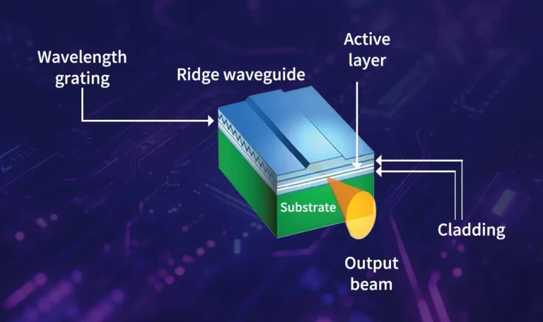
Detailed Introduction to Distributed Feedback (DFB) Laser Chips
2025-12-11
In 2025, the amount of data moving around the world keeps growing very fast. When you build fast 100G...
Quartz Cover Plate vs Regular Glass – Which One Destroys Your Overlay Accuracy
2025-12-05
You’re racing to qualify a MEMS pressure sensor or a LiDAR module, and everything looks perfect until...
Critical Technical Parameters for Precision in Semiconductor Equipment Design
2025-12-04
As the semiconductor field moves to better nodes, mixed integration, and fast applications, the work...
What Is the Essential Carrier Difference from Raw Wafer to Final Chip
2025-11-28
In the complicated world of semiconductor production, a successful output often relies on one simple...
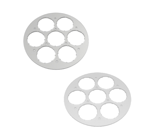
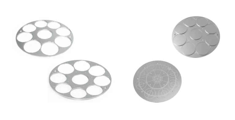
How to Custom Wafer Carrier Trays for Compound Semiconductor Wafers
2025-11-27
Many new industries are growing fast today because of special materials. These include 5G networks, Electric...
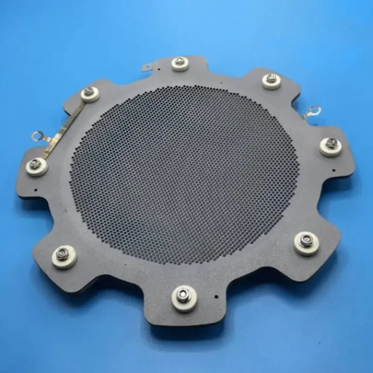
Ion Source Grids in Semiconductor Etching: Boosting Yield and Efficiency
2025-11-21
Etch precision defines your fab’s success. One micron of non-uniformity can scrap an entire wafer. Ion...
Quartz Cover Plate: Equivalent RF Energy Transfer for Uniform Plasma Processing
2025-11-20
Uniform plasma processing decides whether your wafers succeed or fail in high-volume production. Tiny...
1
2
3
4
5
6
7
8
9
10
11
12
13
14